- 您现在的位置:买卖IC网 > PDF目录25646 > SPC563M64L5COAY (STMICROELECTRONICS) 32-BIT, FLASH, 80 MHz, MICROCONTROLLER, PQFP144 PDF资料下载
参数资料
| 型号: | SPC563M64L5COAY |
| 厂商: | STMICROELECTRONICS |
| 元件分类: | 微控制器/微处理器 |
| 英文描述: | 32-BIT, FLASH, 80 MHz, MICROCONTROLLER, PQFP144 |
| 封装: | 20 X 20 MM, LEAD FREE, LQFP-144 |
| 文件页数: | 113/140页 |
| 文件大小: | 1310K |
| 代理商: | SPC563M64L5COAY |
第1页第2页第3页第4页第5页第6页第7页第8页第9页第10页第11页第12页第13页第14页第15页第16页第17页第18页第19页第20页第21页第22页第23页第24页第25页第26页第27页第28页第29页第30页第31页第32页第33页第34页第35页第36页第37页第38页第39页第40页第41页第42页第43页第44页第45页第46页第47页第48页第49页第50页第51页第52页第53页第54页第55页第56页第57页第58页第59页第60页第61页第62页第63页第64页第65页第66页第67页第68页第69页第70页第71页第72页第73页第74页第75页第76页第77页第78页第79页第80页第81页第82页第83页第84页第85页第86页第87页第88页第89页第90页第91页第92页第93页第94页第95页第96页第97页第98页第99页第100页第101页第102页第103页第104页第105页第106页第107页第108页第109页第110页第111页第112页当前第113页第114页第115页第116页第117页第118页第119页第120页第121页第122页第123页第124页第125页第126页第127页第128页第129页第130页第131页第132页第133页第134页第135页第136页第137页第138页第139页第140页
SPC563M64
Electrical characteristics
Doc ID 14642 Rev 6
3.3.1
General notes for specifications at maximum junction temperature
An estimation of the chip junction temperature, TJ, can be obtained from the equation:
Equation 1
TJ = TA + (RθJA * PD)
where:
TA = ambient temperature for the package (
oC)
RθJA = junction-to-ambient thermal resistance (
oC/W)
PD = power dissipation in the package (W)
The thermal resistance values used are based on the JEDEC JESD51 series of standards
to provide consistent values for estimations and comparisons. The difference between the
values determined for the single-layer (1s) board compared to a four-layer board that has
two signal layers, a power and a ground plane (2s2p), demonstrate that the effective thermal
resistance is not a constant. The thermal resistance depends on the:
●
Construction of the application board (number of planes)
●
Effective size of the board which cools the component
●
Quality of the thermal and electrical connections to the planes
●
Power dissipated by adjacent components
Connect all the ground and power balls to the respective planes with one via per ball. Using
fewer vias to connect the package to the planes reduces the thermal performance. Thinner
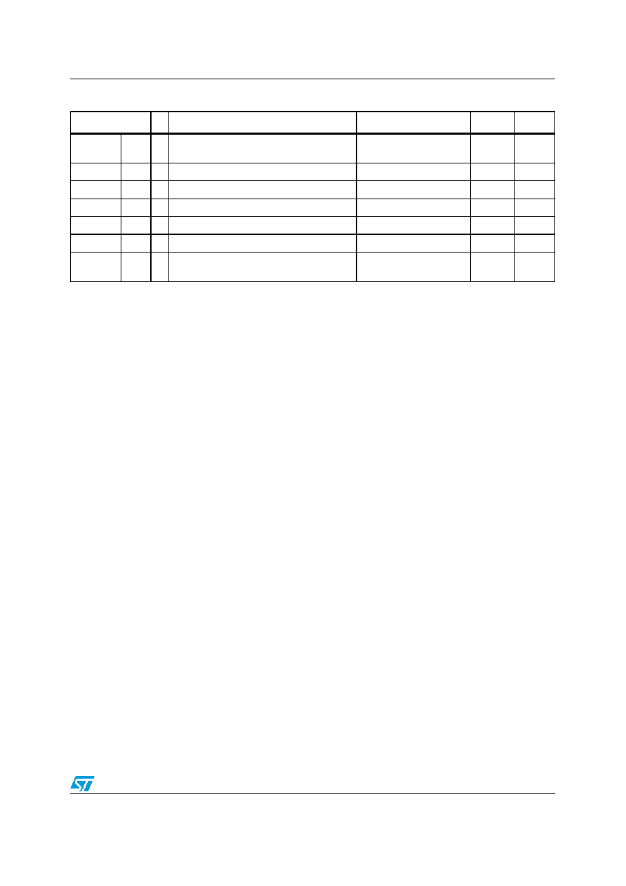
Table 13.
Thermal characteristics for 208-pin LBGA(1)
1.
Thermal characteristics are targets based on simulation that are subject to change per device characterization.
Symbol
C
Parameter
Conditions
Value
Unit
RθJA
CC
D
Junction-to-ambient, natural
convection(2),(3)
2.
Junction temperature is a function of die size, on-chip power dissipation, package thermal resistance, mounting site (board)
temperature, ambient temperature, air flow, power dissipation of other components on the board, and board thermal
resistance.
3.
Per SEMI G38-87 and JEDEC JESD51-2 with the single-layer board horizontal.
One layer board - 1s
39
°C/W
RθJMA
CC
D Junction-to-ambient natural convection(2),(4)
4.
Per JEDEC JESD51-6 with the board horizontal.
Four layer board - 2s2p
24
°C/W
RθJA
CC
D Junction-to-ambient (@200 ft/min)(2),(4)
Single layer board
31
°C/W
RθJMA
CC
D Junction-to-ambient (@200 ft/min)(2),(4)
Four layer board 2s2p
20
°C/W
RθJB
CC
D Junction-to-board(5)
5.
Thermal resistance between the die and the printed circuit board per JEDEC JESD51-8. Board temperature is measured
on the top surface of the board near the package.
Four layer board - 2s2p
13
°C/W
RθJC
CC
D Junction-to-case(6)
6.
Indicates the average thermal resistance between the die and the case top surface as measured by the cold plate method
(MIL SPEC-883 Method 1012.1) with the cold plate temperature used for the case temperature.
6°C/W
ΨJT
CC
D
Junction-to-package top natural
convection(7)
7.
Thermal characterization parameter indicating the temperature difference between package top and the junction
temperature per JEDEC JESD51-2. When Greek letters are not available, the thermal characterization parameter is written
as Psi-JT.
2°C/W
相关PDF资料 |
PDF描述 |
|---|---|
| SPL2Y81 | 808 nm, LASER DIODE |
| SPL2Y98 | 975 nm, LASER DIODE |
| SPLBS79 | LASER DIODE |
| SPLEB98-E | 975 nm, LASER DIODE |
| SPLQY81 | 808 nm, LASER DIODE |
相关代理商/技术参数 |
参数描述 |
|---|---|
| SPC563M64L7COAR | 功能描述:32位微控制器 - MCU 32-BIT Embedded MCU 80 MHz, 1.5 Mbyte RoHS:否 制造商:Texas Instruments 核心:C28x 处理器系列:TMS320F28x 数据总线宽度:32 bit 最大时钟频率:90 MHz 程序存储器大小:64 KB 数据 RAM 大小:26 KB 片上 ADC:Yes 工作电源电压:2.97 V to 3.63 V 工作温度范围:- 40 C to + 105 C 封装 / 箱体:LQFP-80 安装风格:SMD/SMT |
| SPC563M64L7COAY | 制造商:STMicroelectronics 功能描述:JDP MICRO - Bulk |
| SPC563M64L7-ENG | 制造商:STMicroelectronics 功能描述:ENG SAMPLES - Bulk |
| SPC563MADPT144S | 功能描述:32位微控制器 - MCU Socketed Mini Mod SPC563M QFP144 RoHS:否 制造商:Texas Instruments 核心:C28x 处理器系列:TMS320F28x 数据总线宽度:32 bit 最大时钟频率:90 MHz 程序存储器大小:64 KB 数据 RAM 大小:26 KB 片上 ADC:Yes 工作电源电压:2.97 V to 3.63 V 工作温度范围:- 40 C to + 105 C 封装 / 箱体:LQFP-80 安装风格:SMD/SMT |
| SPC563MADPT176S | 功能描述:32位微控制器 - MCU Socketed Mini Mod SPC563M QFP176 RoHS:否 制造商:Texas Instruments 核心:C28x 处理器系列:TMS320F28x 数据总线宽度:32 bit 最大时钟频率:90 MHz 程序存储器大小:64 KB 数据 RAM 大小:26 KB 片上 ADC:Yes 工作电源电压:2.97 V to 3.63 V 工作温度范围:- 40 C to + 105 C 封装 / 箱体:LQFP-80 安装风格:SMD/SMT |
发布紧急采购,3分钟左右您将得到回复。