- 您现在的位置:买卖IC网 > PDF目录25646 > SPC563M64L5COAY (STMICROELECTRONICS) 32-BIT, FLASH, 80 MHz, MICROCONTROLLER, PQFP144 PDF资料下载
参数资料
| 型号: | SPC563M64L5COAY |
| 厂商: | STMICROELECTRONICS |
| 元件分类: | 微控制器/微处理器 |
| 英文描述: | 32-BIT, FLASH, 80 MHz, MICROCONTROLLER, PQFP144 |
| 封装: | 20 X 20 MM, LEAD FREE, LQFP-144 |
| 文件页数: | 135/140页 |
| 文件大小: | 1310K |
| 代理商: | SPC563M64L5COAY |
第1页第2页第3页第4页第5页第6页第7页第8页第9页第10页第11页第12页第13页第14页第15页第16页第17页第18页第19页第20页第21页第22页第23页第24页第25页第26页第27页第28页第29页第30页第31页第32页第33页第34页第35页第36页第37页第38页第39页第40页第41页第42页第43页第44页第45页第46页第47页第48页第49页第50页第51页第52页第53页第54页第55页第56页第57页第58页第59页第60页第61页第62页第63页第64页第65页第66页第67页第68页第69页第70页第71页第72页第73页第74页第75页第76页第77页第78页第79页第80页第81页第82页第83页第84页第85页第86页第87页第88页第89页第90页第91页第92页第93页第94页第95页第96页第97页第98页第99页第100页第101页第102页第103页第104页第105页第106页第107页第108页第109页第110页第111页第112页第113页第114页第115页第116页第117页第118页第119页第120页第121页第122页第123页第124页第125页第126页第127页第128页第129页第130页第131页第132页第133页第134页当前第135页第136页第137页第138页第139页第140页
SPC563M64
Electrical characteristics
Doc ID 14642 Rev 6
—
CC
C
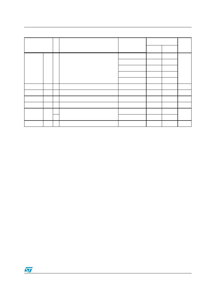
XTAL load capacitance(12)
4MHz
5
30
pF
8MHz
5
26
12 MHz
5
23
16 MHz
5
19
20 MHz
5
16
tlpll
CC
C
PLL lock time (12), (16)
—
200
μs
tdc
CC
C
Duty cycle of reference
—40
60
%
fLCK
CC
C
Frequency LOCK range
—
–6
6
% fsys
fUL
CC
C
Frequency un-LOCK range
—
–18
18
% fsys
fCS
fDS
CC
C
Modulation Depth
Center spread
±0.25
±4.0
%fsys
C
Down Spread
–0.5
–8.0
fMOD
CC
C
Modulation frequency(17)
—
100
kHz
1.
All values given are initial design targets and subject to change. The values in the table are simulated at (VDDPLL =1.14 V to
1.32 V, VSS = VSSPLL = 0 V, TA = TL to TH)
2.
Considering operation with PLL not bypassed.
3.
fVCO is calculated as follows:
— In Legacy Mode fVCO = (fcrystal/(PREDIV+1))*(4*(MFD+4))
— In Enhanced Mode fvco = (fcrystal/(EPREDIV+1))*(EMFD+4)
4.
All internal registers retain data at 0 Hz.
5.
“Loss of Reference Frequency” window is the reference frequency range outside of which the PLL is in self clocked mode.
6.
Self clocked mode frequency is the frequency that the PLL operates at when the reference frequency falls outside the fLOR
window.
7.
fVCO self clock range is 20–150 MHz. fSCM represents fSYS after PLL output divider (ERFD) of 2 through 16 in enhanced
mode.
8.
This value is determined by the crystal manufacturer and board design.
9.
Jitter is the average deviation from the programmed frequency measured over the specified interval at maximum fSYS.
Measurements are made with the device powered by filtered supplies and clocked by a stable external clock signal. Noise
injected into the PLL circuitry via VDDPLL and VSSPLL and variation in crystal oscillator frequency increase the CJITTER
percentage for a given interval.
10. Proper PC board layout procedures must be followed to achieve specifications.
11. Values are with frequency modulation disabled. If frequency modulation is enabled, jitter is the sum of CJITTER and either
fCS or fDS (depending on whether center spread or down spread modulation is enabled).
12. This value is determined by the crystal manufacturer and board design. For 4 MHz to 20 MHz crystals specified for this
PLL, load capacitors should not exceed these limits. For a 20 MHz crystal the maximum load should be 17 pF.
13. Proper PC board layout procedures must be followed to achieve specifications.
14. This parameter is guaranteed by design rather than 100% tested.
15. VIHEXT cannot exceed VRC33 in external reference mode.
16. This specification applies to the period required for the PLL to relock after changing the MFD frequency control bits in the
synthesizer control register (SYNCR).
17. Modulation depth will be attenuated from depth setting when operating at modulation frequencies above 50kHz.
Table 26.
PLLMRFM electrical specifications(1) (continued)
Symbol
C
Parameter
Conditions
Value
Unit
min
max
相关PDF资料 |
PDF描述 |
|---|---|
| SPL2Y81 | 808 nm, LASER DIODE |
| SPL2Y98 | 975 nm, LASER DIODE |
| SPLBS79 | LASER DIODE |
| SPLEB98-E | 975 nm, LASER DIODE |
| SPLQY81 | 808 nm, LASER DIODE |
相关代理商/技术参数 |
参数描述 |
|---|---|
| SPC563M64L7COAR | 功能描述:32位微控制器 - MCU 32-BIT Embedded MCU 80 MHz, 1.5 Mbyte RoHS:否 制造商:Texas Instruments 核心:C28x 处理器系列:TMS320F28x 数据总线宽度:32 bit 最大时钟频率:90 MHz 程序存储器大小:64 KB 数据 RAM 大小:26 KB 片上 ADC:Yes 工作电源电压:2.97 V to 3.63 V 工作温度范围:- 40 C to + 105 C 封装 / 箱体:LQFP-80 安装风格:SMD/SMT |
| SPC563M64L7COAY | 制造商:STMicroelectronics 功能描述:JDP MICRO - Bulk |
| SPC563M64L7-ENG | 制造商:STMicroelectronics 功能描述:ENG SAMPLES - Bulk |
| SPC563MADPT144S | 功能描述:32位微控制器 - MCU Socketed Mini Mod SPC563M QFP144 RoHS:否 制造商:Texas Instruments 核心:C28x 处理器系列:TMS320F28x 数据总线宽度:32 bit 最大时钟频率:90 MHz 程序存储器大小:64 KB 数据 RAM 大小:26 KB 片上 ADC:Yes 工作电源电压:2.97 V to 3.63 V 工作温度范围:- 40 C to + 105 C 封装 / 箱体:LQFP-80 安装风格:SMD/SMT |
| SPC563MADPT176S | 功能描述:32位微控制器 - MCU Socketed Mini Mod SPC563M QFP176 RoHS:否 制造商:Texas Instruments 核心:C28x 处理器系列:TMS320F28x 数据总线宽度:32 bit 最大时钟频率:90 MHz 程序存储器大小:64 KB 数据 RAM 大小:26 KB 片上 ADC:Yes 工作电源电压:2.97 V to 3.63 V 工作温度范围:- 40 C to + 105 C 封装 / 箱体:LQFP-80 安装风格:SMD/SMT |
发布紧急采购,3分钟左右您将得到回复。