- 您现在的位置:买卖IC网 > PDF目录98141 > SPL505YC264ATT PROC SPECIFIC CLOCK GENERATOR, PDSO64 PDF资料下载
参数资料
| 型号: | SPL505YC264ATT |
| 元件分类: | 时钟产生/分配 |
| 英文描述: | PROC SPECIFIC CLOCK GENERATOR, PDSO64 |
| 封装: | 6 X 17 MM, LEAD FREE, MO-153, TSSOP-64 |
| 文件页数: | 23/27页 |
| 文件大小: | 314K |
| 代理商: | SPL505YC264ATT |
第1页第2页第3页第4页第5页第6页第7页第8页第9页第10页第11页第12页第13页第14页第15页第16页第17页第18页第19页第20页第21页第22页当前第23页第24页第25页第26页第27页
SPL505YC264BT
Rev 1.4 May 21, 2007
Page 5 of 27
Frequency Select Pin (FSA, FSB, and FSC)
To achieve host clock frequency selection, apply the appro-
priate logic levels to FS_A, FS_B, and FS_C, inputs before
CK_PWRGD assertion (as seen by the clock synthesizer).
When CK_PWRGD is sampled HIGH by the clock chip
(indicating processor CK_PWRGD voltage is stable), the clock
chip samples the FS_A, FS_B, and FS_C, input values. For all
logic levels of FS_A, FS_B, and FS_C CK_PWRGDemploys
a one-shot functionality, in that once a valid HIGH on
CK_PWRGD has been sampled, all further CK_PWRGD
FS_A, FS_B, and FS_C, transitions will be ignored, except in
test mode.
Serial Data Interface
To enhance the flexibility and function of the clock synthesizer,
a two-signal serial interface is provided. Through the Serial
Data Interface, various device functions, such as individual
clock output buffers, can be individually enabled or disabled.
The registers associated with the Serial Data Interface
initialize to their default setting upon power-up, and therefore
use of this interface is optional. Clock device register changes
are normally made upon system initialization, if any are
required. The interface cannot be used during system
operation for power management functions.
Data Protocol
The clock driver serial protocol accepts byte write, byte read,
block write, and block read operations from the controller. For
block write/read operation, the bytes must be accessed in
sequential order from lowest to highest byte (most significant
bit first) with the ability to stop after any complete byte has
been transferred. For byte write and byte read operations, the
system controller can access individually indexed bytes. The
offset of the indexed byte is encoded in the command code,
as described in Table 2.
The block write and block read protocol is outlined in Table 3
while Table 4 outlines the corresponding byte write and byte
read protocol. The slave receiver address is 11010010 (D2h)
.
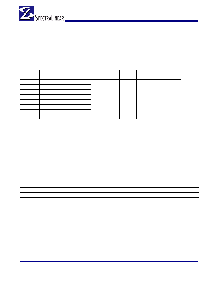
Frequency Select Pin (FSA, FSB, and FSC)
Input Conditions
Output Frequency
FSC
FSB
FSA
CPU
(MHz)
SRC
(MHz)
SATA
(MHz)
DOT96
(MHz)
USB
(MHz)
PCI
(MHz)
REF
(MHz)
FSEL_2
FSEL_1
FSEL_0
1
0
1
100
96
48
33.3
14.318
0
1
133
0
1
166
0
1
0
200
0
266
1
0
333
1
0
400
1
200
Table 2. Command Code Definition
Bit
Description
7
0 = Block read or block write operation, 1 = Byte read or byte write operation
(6:0)
Byte offset for byte read or byte write operation. For block read or block write operations, these bits should be
'0000000'
相关PDF资料 |
PDF描述 |
|---|---|
| SPL505YC264BT | 400 MHz, PROC SPECIFIC CLOCK GENERATOR, PDSO64 |
| SPL505YC264BT | 400 MHz, PROC SPECIFIC CLOCK GENERATOR, PDSO64 |
| SPW08F0D | SINGLE COLOR LED, PURE WHITE, 3.5 mm |
| SSC-SFT825N-S | TRIPLE COLOR LED, RED/GREEN/BLUE, 2.4 mm |
| SSI32C452-CP | 20 Mbps, ST506; ST412; ST412HP; SA100 COMPATIBLE, FIXED DISK CONTROLLER, PDIP40 |
相关代理商/技术参数 |
参数描述 |
|---|---|
| SPL505YC264BT | 功能描述:时钟发生器及支持产品 CK505 v0.85 RoHS:否 制造商:Silicon Labs 类型:Clock Generators 最大输入频率:14.318 MHz 最大输出频率:166 MHz 输出端数量:16 占空比 - 最大:55 % 工作电源电压:3.3 V 工作电源电流:1 mA 最大工作温度:+ 85 C 安装风格:SMD/SMT 封装 / 箱体:QFN-56 |
| SPL505YC264BTT | 功能描述:时钟发生器及支持产品 CK505 v0.85 RoHS:否 制造商:Silicon Labs 类型:Clock Generators 最大输入频率:14.318 MHz 最大输出频率:166 MHz 输出端数量:16 占空比 - 最大:55 % 工作电源电压:3.3 V 工作电源电流:1 mA 最大工作温度:+ 85 C 安装风格:SMD/SMT 封装 / 箱体:QFN-56 |
| SPL5100PT | 制造商:CHENMKO 制造商全称:Chenmko Enterprise Co. Ltd. 功能描述:SCHOTTKY BARRIER RECTIFIER |
| SPL520LLPT | 制造商:CHENMKO 制造商全称:Chenmko Enterprise Co. Ltd. 功能描述:SCHOTTKY BARRIER RECTIFIER |
| SPL53-1024 | 制造商:Power-One 功能描述: |
发布紧急采购,3分钟左右您将得到回复。