- 您现在的位置:买卖IC网 > PDF目录9603 > SPL505YC264BTT (Silicon Laboratories Inc)IC CLOCK CK505 BEARLAKE 64TSSOP PDF资料下载
参数资料
| 型号: | SPL505YC264BTT |
| 厂商: | Silicon Laboratories Inc |
| 文件页数: | 12/27页 |
| 文件大小: | 0K |
| 描述: | IC CLOCK CK505 BEARLAKE 64TSSOP |
| 标准包装: | 2,000 |
| 类型: | 时钟/频率发生器,多路复用器 |
| PLL: | 是 |
| 主要目的: | Intel CPU,PCI Express(PCIe) |
| 输入: | 晶体 |
| 输出: | LVCMOS |
| 电路数: | 1 |
| 比率 - 输入:输出: | 1:22 |
| 差分 - 输入:输出: | 无/是 |
| 频率 - 最大: | 400MHz |
| 电源电压: | 3.135 V ~ 3.465 V |
| 工作温度: | 0°C ~ 85°C |
| 安装类型: | * |
| 封装/外壳: | * |
| 供应商设备封装: | * |
| 包装: | * |
第1页第2页第3页第4页第5页第6页第7页第8页第9页第10页第11页当前第12页第13页第14页第15页第16页第17页第18页第19页第20页第21页第22页第23页第24页第25页第26页第27页
SPL505YC26
......................Document #: 001-03543 Rev *E Page 2 of 27
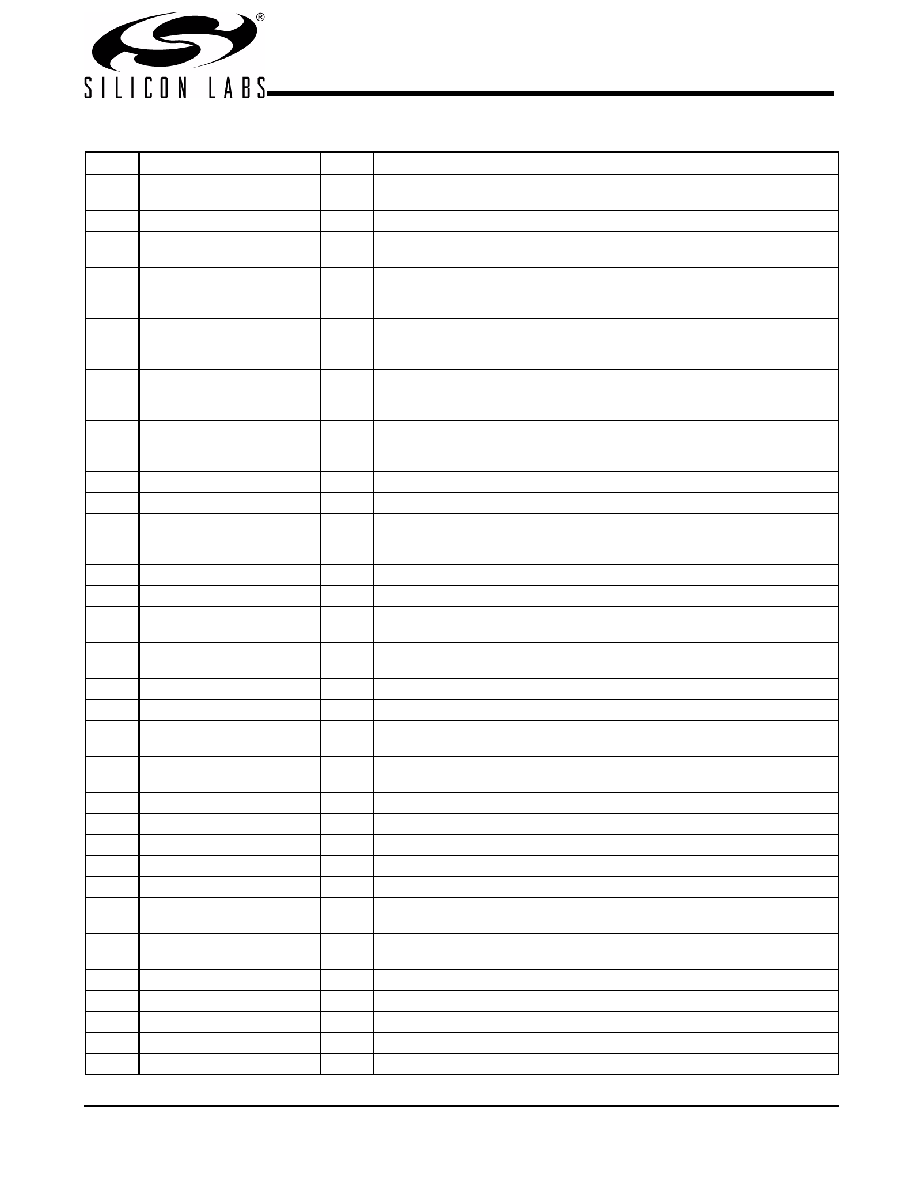
Pin Definitions
Pin No.
Name
Type
Description
1
PCI_0/OE#_0/2_A
I/O, SE 33 MHz clock/3.3V OE# Input mappable via I2C to control either SRC 0 or
SRC 2. Default PCI0
2
VDD_PCI
PWR
3.3V Power supply for PCI PLL.
3
PCI_1/OE#_1/4_A
I/O, SE 33 MHz clock/3.3V OE# Input mappable via I2C to control either SRC 1 or
SRC 4. Default PCI1.
4
PCI_2/TME
I/O, SE 3.3V tolerance input for overclocking enable pin 33 MHz clock.
Refer to DC Electrical Specifications table for Vil_FS and Vih_FS specifica-
tions.
5
PCI_3/CFG0
I/O, SE,
PD
3.3V tolerant input for CPU frequency selection/33 MHz clock.
Refer to DC Electrical Specifications table for Vil_PCI3/CFG0 and
Vih_PCI3/CFG0 specifications.
6
PCI_4/SRC5_SEL
I/O, SE 3.3V tolerant input to enable SRC5/33 MHz clock output.
(sampled on the CK_PWRGD assertion)
1 = SRC5, 0 = CPU_STOP#
7
PCIF_0/ITP_EN
I/O, SE 3.3V LVTTL input to enable SRC8 or CPU2_ITP/33 MHz clock output.
(sampled on the CK_PWRGD assertion)
1 = CPU2_ITP, 0 = SRC8
8
VSS_PCI
GND
Ground for outputs.
9
VDD_48
PWR
3.3V Power supply for outputs and PLL.
10
USB_48/FSA
I/O
3.3V tolerant input for CPU frequency selection/fixed 48 MHz clock output.
Refer to DC Electrical Specifications table for Vil_FS and Vih_FS specifica-
tions.
11
VSS_48
GND
Ground for outputs.
12
VDD_IO
PWR
0.7V Power supply for outputs.
13
SRC0/DOT96T
O, DIF 100 MHz Differential serial reference clocks/Fixed 96 MHz clock output.
Selected via I2C default is SRC0.
14
SRC0#/DOT96#
O, DIF 100 MHz Differential serial reference clocks/Fixed 96 MHz clock output.
Selected via I2C default is SRC0.
15
VSS_IO
GND
Ground for PLL2.
16
VDD_PLL3
PWR
3.3V Power supply for PLL3
17
SRC1/LCD_100/SE1
O, DIF,
SE
100 MHz Differential serial reference clocks/100 MHz LCD video clock/SE1
clocks. Default SRC1
18
SRC1#/LCD_100#/SE2
O, DIF,
SE
100 MHz Differential serial reference clocks/100 MHz LCD video clock/SE2
clocks. Default SRC1
19
VSS_PLL3
GND
Ground for PLL3.
20
VDD_PLL3_IO
PWR
0.7V Power supply for PLL3 outputs.
21
SRC2/SATA
O, DIF 100 MHz Differential serial reference clocks.
22
SRC2#/SATA#
O, DIF 100 MHz Differential serial reference clocks.
23
VSS_SRC
GND
Ground for outputs.
24
SRC3/OE#_0/2_B
I/O,
Dif
100-MHz Differential serial reference clocks / 3.3V OE#_0/2_B, input,
mappable via I2C to control either SRC 0 or SRC 2. Default SRC3
25
SRC3#OE#_1/4_B
I/O,
Dif
100-MHz Differential serial reference clocks / 3.3V OE#_1/4_B input,
mappable via I2C to control either SRC 1 or SRC 4. Default SRC3
26
VDD_SRC_IO
PWR
0.7V power supply for SRC outputs.
27
SRC4
O, DIF 100 MHz Differential serial reference clocks.
28
SRC4#
O, DIF 100 MHz Differential serial reference clocks.
29
VSS_SRC
GND
Ground for outputs.
30
SRC9
O, DIF 100 MHz Differential serial reference clocks.
相关PDF资料 |
PDF描述 |
|---|---|
| D38999/26JE26JA | CONN PLUG 26POS STRAIGHT W/SCKT |
| V24B28H250B3 | CONVERTER MOD DC/DC 28V 250W |
| ICS932S200BFLFT | IC FREQ TIMING GENERATOR 56-SSOP |
| MS27473E24B4S | CONN PLUG 56POS STRAIGHT W/SCKT |
| V24B24H250BG2 | CONVERTER MOD DC/DC 24V 250W |
相关代理商/技术参数 |
参数描述 |
|---|---|
| SPL5100PT | 制造商:CHENMKO 制造商全称:Chenmko Enterprise Co. Ltd. 功能描述:SCHOTTKY BARRIER RECTIFIER |
| SPL520LLPT | 制造商:CHENMKO 制造商全称:Chenmko Enterprise Co. Ltd. 功能描述:SCHOTTKY BARRIER RECTIFIER |
| SPL53-1024 | 制造商:Power-One 功能描述: |
| SPL53-4000 | 制造商:Power-One 功能描述: |
| SPL-53-DR-IR1-CDA | 制造商:SOURCE 制造商全称:Source Photonics, Inc. 功能描述:SFP Bi-Directional Transceiver Preliminary |
发布紧急采购,3分钟左右您将得到回复。