参数资料
| 型号: | SSM2018PZ |
| 厂商: | Analog Devices Inc |
| 文件页数: | 15/16页 |
| 文件大小: | 0K |
| 描述: | IC AMP AUDIO MONO CLASS AB 16DIP |
| 标准包装: | 25 |
| 放大器类型: | 音频 |
| 电路数: | 1 |
| 转换速率: | 5 V/µs |
| 增益带宽积: | 14MHz |
| 电流 - 输入偏压: | 250nA |
| 电压 - 输入偏移: | 1000µV |
| 电流 - 电源: | 11mA |
| 电压 - 电源,单路/双路(±): | 10 V ~ 36 V,±5 V ~ 18 V |
| 工作温度: | -40°C ~ 85°C |
| 安装类型: | 通孔 |
| 封装/外壳: | 16-DIP(0.300",7.62mm) |
| 供应商设备封装: | 16-PDIP |
| 包装: | 管件 |
| 产品目录页面: | 775 (CN2011-ZH PDF) |
REV. B
–8–
SSM2018T
normal and actually disables that output amplifier ensuring that
it will not oscillate and cause interference problems. Shorting
the output to the negative supply does not cause the supply
current to increase. This amplifier is only used in the “OVCE”
application explained later.
The control port follows a –30 mV/dB control law. The applica-
tion circuit shows a 3 k
W and 1 kW resistor divider from a control
voltage. The choice of these resistors is arbitrary and could be
any values to properly scale the control voltage. In fact, these
resistors can be omitted if the control voltage has been properly
scaled. The 1
mF capacitor is in place to provide some filtering
of the control signal. Although the control feedthrough is trimmed
at the factory, the feedthrough increases with frequency (TPC
16). Thus, high frequency noise can feed through and add to
the noise of the VCA. Filtering the control signal helps minimize
this noise source.
Theory of Operation of the SSM2018T
The SSM2018T has the same internal circuitry as the original
SSM2018. The detailed diagram in Figure 2 shows the main
components of the VCA. The essence of the SSM2018T is
the gain core, which comprises two differential pairs (Q1–Q4).
When the control voltage, VC, is adjusted, current through the
gain core is steered to one side or the other of the two differential
pairs. The tail current for these differential pairs is set by the
mode bias of the VCA (Class A or AB), which is labeled as IM in
the diagram. IM is then modulated by a current proportional to
the input voltage, labeled IS. For a positive input voltage, more
current is steered (by the “Splitter”) to the left differential pair;
the opposite is true for a negative input.
To understand how the gain control works, a simple example is
best. Take the case of a positive control voltage on Pin 11. Notice
that the bases of Q2 and Q3 are connected to ground via a 200
W resistor. A positive control voltage produces a positive voltage
on the bases of Q1 and Q4. Concentrating on the left-most
differential pair, this raises the base voltage of Q1 above that of
Q2. Thus, more of the tail current is steered through Q1 than
through Q2. The current from the collector of Q2 flows through
the external 18 k
W feedback resistor around amplifier A3. When
this current is reduced, the output voltage is also reduced. Thus,
a positive control voltage results in an attenuation of the input
signal, which explains why the gain constant is negative.
The collector currents of Q2 and Q3 produce the output voltage.
The output of Q3 is mirrored by amplifier A1 to add to the
overall output voltage. On the other hand, the collector currents
of Q1 and Q4 are used for feedback to the differential inputs.
Because Pins 6 and 4 are shorted together, any input voltage
produces an input current which flows into Pin 4. The same is
true for the inverting input, which is connected to Pin 1. The
overall feedback ensures that the current flowing through the
input resistors is balanced by the collector currents in Q1 and Q4.
Compensating the SSM2018T
The SSM108 has a network that uses an adaptive compensation
scheme that adjusts the optimum compensation level for a given
gain. The control voltage not only adjusts the gain core steering,
it also adjusts the compensation. The SSM2018T has three
compensation pins: COMP1, COMP2, and COMP3. COMP3
is normally left open. Grounding this pin actually defeats the adap-
tive compensation circuitry, giving the VCA a fixed compensation
point. The only time this is desirable is when the VCA has fixed
feedback, such as the Voltage Controlled Panner (VCP) circuit
APPLICATIONS
The SSM2018T is a trimless Voltage Controlled Amplifier (VCA)
for volume control in audio systems. The SSM2018T is identi-
cal to the original SSM2018 in functionality and pinout; how-
ever, it is the first professional quality audio VCA in the
marketplace that does not require an external trimming potenti-
ometer to minimize distortion. Instead, the SSM2018T is laser
trimmed before it is packaged to ensure the specified THD and
control feedthrough performance. This has a significant savings
in not only the cost of external trimming potentiometers, but
also the manufacturing cost of performing the trimming during
production.
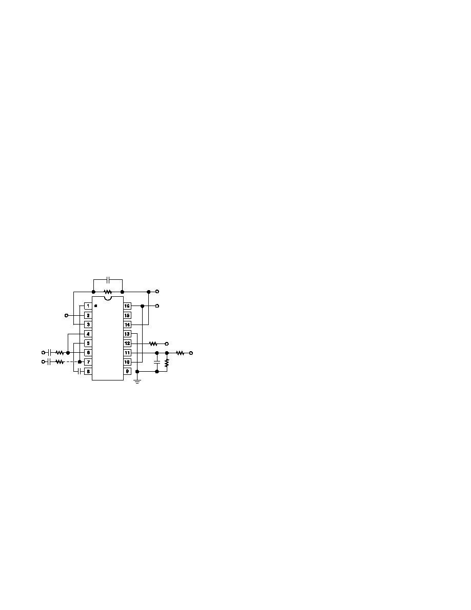
Basic VCA Configuration
The primary application circuit for the SSM2018T is the basic
VCA configuration, which is shown in Figure 1. This configura-
tion uses differential current feedback to realize the VCA. A
complete description of the internal circuitry of the VCA, and
this configuration, is given in the Theory of Operation section
below. The SSM2018T is trimmed at the factory for operation in the
basic VCA configuration with class AB biasing. Thus, for optimal
distortion and control feedthrough performance, the same con-
figuration and biasing should be used. All of the graphs for the
SSM2018T in the data sheet have been measured using the
circuit of Figure 1.
V+
1 F
RB
150k
18k
V+
18k
VIN+
1 F 18k
VIN–
47pF
1 F
50pF
1k
VCONTROL
3k
VOUT
V–
SSM2018T
Figure 1. Basic VCA Application Circuit
In the simple VCA configuration, the SSM2018T inputs are at a
virtual ground. Thus, 18 k
W resistors are required to convert the
input voltages to input currents. The schematic also shows ac
coupling capacitors. These are inserted to minimize dc offsets
generated by bias current through the resistors. Without the
capacitors, the dc offset due to the input bias current is typically
5 mV. The input stage has the flexibility to run either inverting,
noninverting, or balanced. The most common configuration is
to run it in the noninverting single-ended mode. If either input
is unused, the associated 18 k
W resistor and coupling capacitor
should be removed to prevent any additional noise.
The common-mode rejection in balanced mode is typically
55 dB up to 1 kHz, decreasing at higher frequencies as shown in
TPC 21. To ensure good CMRR in the balanced configuration,
the input resistors must be balanced. For example, a 1% mis-
match results in a CMRR of 40 dB. To achieve 55 dB, these
resistors should have an absolute tolerance match of 0.1%.
The output of the basic VCA is taken from Pin 14, which is the
output of an internal amplifier. Notice that the second voltage
output (Pin 16) is connected to the negative supply. This is
相关PDF资料 |
PDF描述 |
|---|---|
| ADA4084-2ARMZ | IC OPAMP GP RRIO 10MHZ DL 8MSOP |
| M83-LML3M1N60-0000-000 | CONN HDR 2MM R/A W/SCREW 60POS |
| LT6600IS8-10#PBF | IC AMP DIFF LP FLTR 10MHZ 8-SOIC |
| LT1368CS8#PBF | IC OP-AMP R-R IN/OUT DUAL 8-SOIC |
| M80-5S22605MQ | CONN HDR 2MM R/A W/SCREW 26POS |
相关代理商/技术参数 |
参数描述 |
|---|---|
| SSM2018PZKL1 | 制造商:Analog Devices 功能描述: |
| SSM2018S | 制造商:AD 制造商全称:Analog Devices 功能描述:Trimless Voltage Controlled Amplifiers |
| SSM2018T | 制造商:AD 制造商全称:Analog Devices 功能描述:Trimless Voltage Controlled Amplifiers |
| SSM2018TN | 制造商:未知厂家 制造商全称:未知厂家 功能描述:Voltage Controlled Gain Amplifier |
| SSM2018TP | 制造商:Analog Devices 功能描述:SP Amp Voltage Controlled Amplifier Single 制造商:Analog Devices 功能描述:AMP VOLT CONTROLLED 2018 DIP16 |
发布紧急采购,3分钟左右您将得到回复。