参数资料
| 型号: | SSM2018PZ |
| 厂商: | Analog Devices Inc |
| 文件页数: | 4/16页 |
| 文件大小: | 0K |
| 描述: | IC AMP AUDIO MONO CLASS AB 16DIP |
| 标准包装: | 25 |
| 放大器类型: | 音频 |
| 电路数: | 1 |
| 转换速率: | 5 V/µs |
| 增益带宽积: | 14MHz |
| 电流 - 输入偏压: | 250nA |
| 电压 - 输入偏移: | 1000µV |
| 电流 - 电源: | 11mA |
| 电压 - 电源,单路/双路(±): | 10 V ~ 36 V,±5 V ~ 18 V |
| 工作温度: | -40°C ~ 85°C |
| 安装类型: | 通孔 |
| 封装/外壳: | 16-DIP(0.300",7.62mm) |
| 供应商设备封装: | 16-PDIP |
| 包装: | 管件 |
| 产品目录页面: | 775 (CN2011-ZH PDF) |
REV. B
–12–
SSM2018T
If a symmetry trim is to be performed, it should precede the
control feedthrough trim and be done as follows:
1. Apply a 1 kHz sine wave of 10 dBu to the input with the
control voltage set for unity gain.
2. Adjust the symmetry trim potentiometer to minimize distor-
tion of the output signal.
Next the control feedthrough trim is done as follows:
1. Ground the input signal port and apply a 60 Hz sine wave
to the control port. The sine wave should have its high and
low peaks correspond to the highest gain to be used in the
application and 30 dB of attenuation, respectively. For
example, a range of 20 dB gain to 30 dB attenuation requires
that the sine wave amplitude ranges between –560 mV and
+840 mV on Pin 11.
2. Adjust the control feedthrough potentiometer to null the
signal seen at the output.
VIN
VC
VG
V1–G
Figure 7. OVCE Follower/VCA Connection
18k
50pF
470k
500k
V+
100k
10M
CONTROL
FEEDTHROUGH
TRIM
V+
V–
V1–G
VG
INPUTS
220pF
NC
V–
1 F
1k
3k
VCONTROL
RB: 30k
FOR CLASS A
150k
FOR CLASS AB
NC = NO CONNECT
SYMMETRY
TRIM
V+
RB
1
2
3
4
5
6
7
8
16
15
14
13
12
11
10
9
SSM2018T
18k
50pF
Figure 8. OVCE Application Circuit
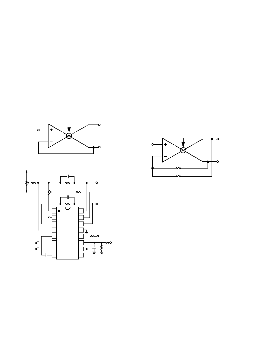
Voltage Controlled Panner
An interesting circuit that is built with the OVCE building
block is a voltage controlled panner. Figure 9 shows the feed-
back connection for the circuit. Notice that the average of both
outputs is fed back to the input. Thus, the average must be
equal to the input voltage. When the control voltage is set for
gain at VG, this causes V1–G to attenuate (to keep the average the
same). On the other hand, when VG is attenuated, V1–G is ampli-
fied. The result is that the control voltage causes the input to
“pan” from one output to the other. The following expressions
show how this circuit works mathematically:
V
G = 2 K V IN and V I –G = 2(1 – K ) V IN
(4)
where K varies between 0 and 1 as the control voltage is changed
from full attenuation to full gain, respectively. When VC = 0,
then K = 0.5 and VG = V1–G = VIN. Again, trimming is required
for best performance. Pin 9 must be grounded. This is possible
because the feedback is constant and the adaptive network is not
needed. The VCP is the only application shown in this data
sheet where Pin 9 is grounded.
VIN
VC
VG
V1–G
18k
Figure 9. Basic VCP Connection
相关PDF资料 |
PDF描述 |
|---|---|
| ADA4084-2ARMZ | IC OPAMP GP RRIO 10MHZ DL 8MSOP |
| M83-LML3M1N60-0000-000 | CONN HDR 2MM R/A W/SCREW 60POS |
| LT6600IS8-10#PBF | IC AMP DIFF LP FLTR 10MHZ 8-SOIC |
| LT1368CS8#PBF | IC OP-AMP R-R IN/OUT DUAL 8-SOIC |
| M80-5S22605MQ | CONN HDR 2MM R/A W/SCREW 26POS |
相关代理商/技术参数 |
参数描述 |
|---|---|
| SSM2018PZKL1 | 制造商:Analog Devices 功能描述: |
| SSM2018S | 制造商:AD 制造商全称:Analog Devices 功能描述:Trimless Voltage Controlled Amplifiers |
| SSM2018T | 制造商:AD 制造商全称:Analog Devices 功能描述:Trimless Voltage Controlled Amplifiers |
| SSM2018TN | 制造商:未知厂家 制造商全称:未知厂家 功能描述:Voltage Controlled Gain Amplifier |
| SSM2018TP | 制造商:Analog Devices 功能描述:SP Amp Voltage Controlled Amplifier Single 制造商:Analog Devices 功能描述:AMP VOLT CONTROLLED 2018 DIP16 |
发布紧急采购,3分钟左右您将得到回复。