参数资料
| 型号: | SSM2018PZ |
| 厂商: | Analog Devices Inc |
| 文件页数: | 16/16页 |
| 文件大小: | 0K |
| 描述: | IC AMP AUDIO MONO CLASS AB 16DIP |
| 标准包装: | 25 |
| 放大器类型: | 音频 |
| 电路数: | 1 |
| 转换速率: | 5 V/µs |
| 增益带宽积: | 14MHz |
| 电流 - 输入偏压: | 250nA |
| 电压 - 输入偏移: | 1000µV |
| 电流 - 电源: | 11mA |
| 电压 - 电源,单路/双路(±): | 10 V ~ 36 V,±5 V ~ 18 V |
| 工作温度: | -40°C ~ 85°C |
| 安装类型: | 通孔 |
| 封装/外壳: | 16-DIP(0.300",7.62mm) |
| 供应商设备封装: | 16-PDIP |
| 包装: | 管件 |
| 产品目录页面: | 775 (CN2011-ZH PDF) |
REV. B
–9–
SSM2018T
A4
Q3
Q4
Q1
Q2
200
1–G
G
1–G
200
1.8k
GAIN
CORE
COMP 1
COMPENSATION
NETWORK
VREF
Im
SPLITTER
A1
A3
VG
+I 1-G
BAL
–I 1-G
V 1-G
V C
GND
MODE
–I G
COMP 3
COMP 2
V+
V–
+IN
–IN
A2
A4
Im + (
)
Is
2
Im – (
)
Is
2
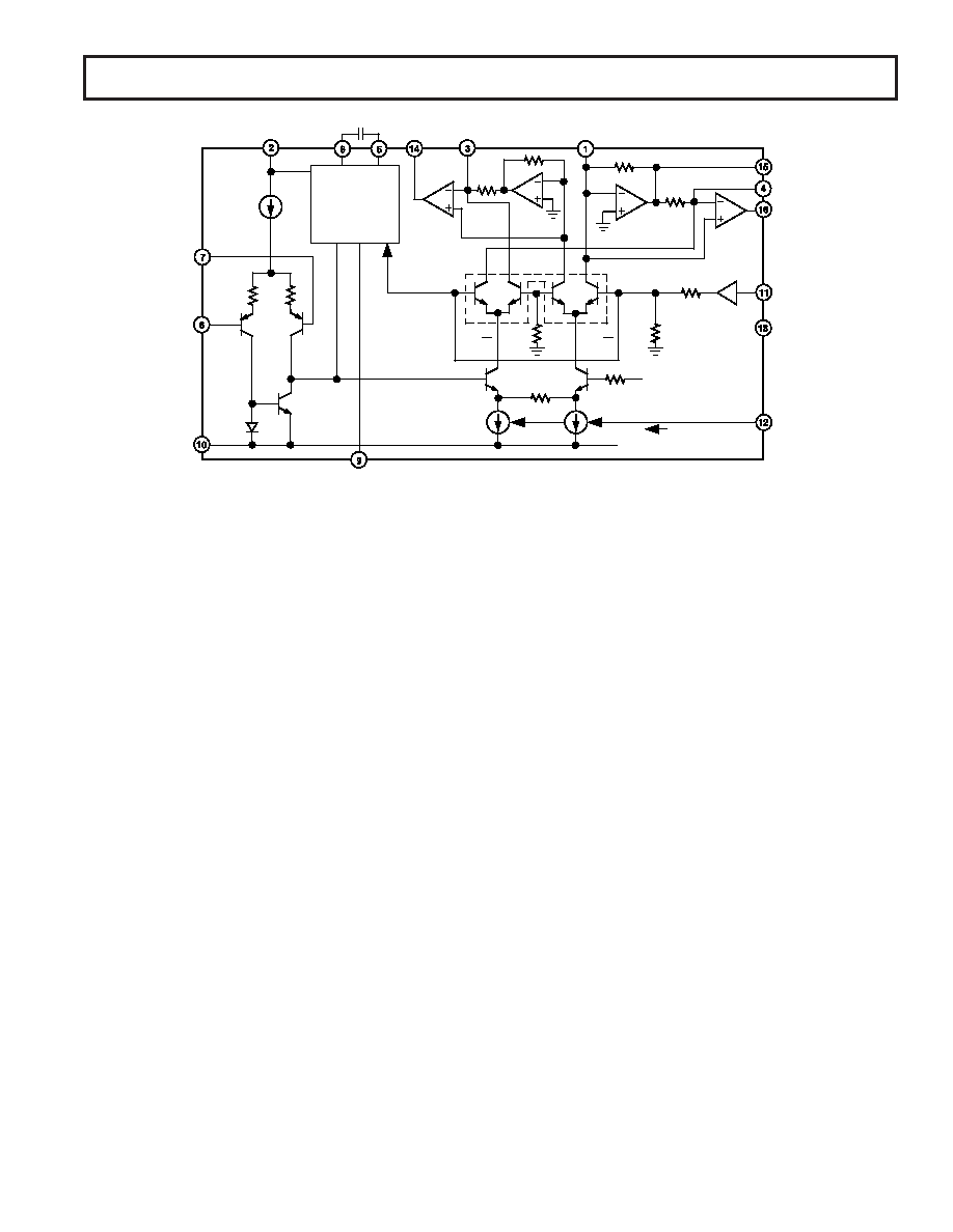
Figure 2. SSM2018T Detailed Functional Diagram
shown later in the data sheet. Thus, for the Basic VCA circuit
or the OVCE circuit, COMP3 should be left open.
A compensation capacitor does need to be added between
COMP1 and COMP2. Because the VCA operates over such a
wide gain range, the compensation should ideally be optimized
for each gain. When the VCA is in high attenuation, there is
very high “loop gain,” and the part needs to have high compen-
sation. On the other hand, at high gain, the same compensation
capacitor would overcompensate the part and roll off the high
frequency performance. Thus, the SSM2018T employs a patented
adaptive compensation circuit. The compensation capacitor is
“Miller” connected between the base and collector of an inter-
nal transistor. By changing the gain of this transistor via the
control voltage, the compensation is changed.
Increasing the compensation capacitor causes the frequency
response and slew rate to decrease, which tends to cause high
frequency distortion to increase. For the basic VCA circuit, 47
pF was chosen as the optimal value. The OVCE circuit described
later uses a 220 pF capacitor. The reason for the increase is to
compensate for the extra phase shift from the additional output
amplifier used in the OVCE configuration. The compensation
capacitor can be adjusted over a practical range from 47 pF to
220 pF if desired. Below 47 pF, the parts may oscillate; above
220 pF the frequency response is significantly degraded.
Control Section
As noted above, the control voltage on Pin 11 steers the current
through the gain core transistors to set the gain. The unity gain
(0 dB) condition occurs at VC = 0. Attenuation occurs in the
VCA for positive voltages (0 V to 3 V, typ), and gain occurs for
negative voltage (0 V to –1.3 V, typ). From –1.3 V to
+3.0 V, 140 dB of gain range is obtainable. The output gain
formula is as follows:
V
OUT = V IN e
(–aV
C )
(1)
The exponential term arises from the standard Ebers-Moll
equation describing the relationship of a transistor’s collector
current as a function of the base-emitter voltage:
IC = IS e(VBE /VT )
(2)
The factor “a” is a function not only of VT but also the scaling
due to the resistor divider of the 200
W and 1.8 kW resistors
shown in Figure 2. The resulting expression for “a” is as follows:
a = 1/(10
V
T), which is approximately equal to 4 at room
temperature. Substituting a = 4 in the above equation results in
a –28.8 mV/dB control law at room temperature.
The –28.8 mV/dB number is slightly different from the data
sheet specification of –30 mV/dB. The difference arises from
the temperature dependency of the control law. The term VT
is known as the thermal voltage, and it has a direct dependency
on temperature: VT = kT/q (k = Boltzmann’s constant =
1.38E–23, q = electron charge = 1.6E–19, and T = absolute
temperature in Kelvin). This temperature dependency leads to
the –3500 ppm/
∞C drift of the control law. It also means that the
control law changes as the part warms up. Thus, our specifica-
tion for the control law states that the part has been powered up
for 60 seconds.
When the part is initially turned on, the temperature of the die
is still at the ambient temperature (25
∞C for example), but the
power dissipation causes the die to warm up. With
±15 V supplies
and a supply current of 11 mA, 330 mW is dissipated. This
number is multiplied by
q
JA to determine the rise in the die’s
temperature. In this case, the die increases from 25
∞C to approxi-
mately 50
∞C. A 25∞C temperature change causes a 8.25%
increase in the gain constant, resulting in a gain constant of 30
mV/dB. The graph in Figure 17 shows how the gain constant
varies over the full temperature range.
相关PDF资料 |
PDF描述 |
|---|---|
| ADA4084-2ARMZ | IC OPAMP GP RRIO 10MHZ DL 8MSOP |
| M83-LML3M1N60-0000-000 | CONN HDR 2MM R/A W/SCREW 60POS |
| LT6600IS8-10#PBF | IC AMP DIFF LP FLTR 10MHZ 8-SOIC |
| LT1368CS8#PBF | IC OP-AMP R-R IN/OUT DUAL 8-SOIC |
| M80-5S22605MQ | CONN HDR 2MM R/A W/SCREW 26POS |
相关代理商/技术参数 |
参数描述 |
|---|---|
| SSM2018PZKL1 | 制造商:Analog Devices 功能描述: |
| SSM2018S | 制造商:AD 制造商全称:Analog Devices 功能描述:Trimless Voltage Controlled Amplifiers |
| SSM2018T | 制造商:AD 制造商全称:Analog Devices 功能描述:Trimless Voltage Controlled Amplifiers |
| SSM2018TN | 制造商:未知厂家 制造商全称:未知厂家 功能描述:Voltage Controlled Gain Amplifier |
| SSM2018TP | 制造商:Analog Devices 功能描述:SP Amp Voltage Controlled Amplifier Single 制造商:Analog Devices 功能描述:AMP VOLT CONTROLLED 2018 DIP16 |
发布紧急采购,3分钟左右您将得到回复。