- 您现在的位置:买卖IC网 > PDF目录10398 > SSM2166SZ-REEL (Analog Devices Inc)IC PREAMP AUDIO MONO MIC 14SOIC PDF资料下载
参数资料
| 型号: | SSM2166SZ-REEL |
| 厂商: | Analog Devices Inc |
| 文件页数: | 4/20页 |
| 文件大小: | 0K |
| 描述: | IC PREAMP AUDIO MONO MIC 14SOIC |
| 产品变化通告: | Material Change 25/Mar/2009 |
| 标准包装: | 1 |
| 类型: | AB 类 |
| 输出类型: | 1-通道(单声道) |
| 电源电压: | 4.5 V ~ 5.5 V |
| 特点: | 麦克风 |
| 安装类型: | 表面贴装 |
| 供应商设备封装: | 14-SOICN |
| 封装/外壳: | 14-SOIC(0.154",3.90mm 宽) |
| 包装: | 标准包装 |
| 产品目录页面: | 775 (CN2011-ZH PDF) |
| 其它名称: | SSM2166SZ-REELDKR |
SSM2166
Data Sheet
Rev. E | Page 12 of 20
POWER-DOWN FEATURE
The supply current of the SSM2166 can be reduced to less than
100 A by applying an active high, 5 V CMOS-compatible input
to the POWER DOWN pin (Pin 12). In this state, the input and
output circuitry of the SSM2166 assumes a high impedance
state; as such, the potentials at the input pin and the output pin are
determined by the external circuitry connected to the SSM2166.
The SSM2166 takes approximately 200 ms to settle from a power-
down to power-on command. For power-on to power-down,
the SSM2166 requires more time, typically less than 1 second.
Cycling the power supply to the SSM2166 can result in quicker
settling times: the off-to-on settling time of the SSM2166 is less
than 200 ms, while the on-to-off settling time is less than 1 ms.
In either implementation, transients may appear at the output of
the device. To avoid these output transients, use mute control of
the VCA gain as previously mentioned.
PCB LAYOUT CONSIDERATIONS
Because the SSM2166 is capable of wide bandwidth operation
and can be configured for as much as 80 dB of gain, special care
must be exercised in the layout of the PCB that contains the IC
and its associated components. The following recommendations
should be considered and/or followed:
In some high system gain applications, the shielding of input
wires to minimize possible feedback from the output of the
SSM2166 back to the input circuit may be necessary.
A single-point (star) ground implementation is recom-
mended in addition to maintaining short lead lengths and
PCB runs. The evaluation board layout shown in Figure 27,
Figure 28, and Figure 29 demonstrates the single-point
grounding scheme. In applications where an analog ground
and a digital ground are available, the SSM2166 and its
surrounding circuitry should be connected to the analog
ground of the system. Because of these recommendations,
wire-wrap board connections and grounding
implementations should be avoided.
The internal buffer of the SSM2166 was designed to drive only
the input of the internal VCA and its own feedback network.
Stray capacitive loading to ground from the BUF OUT pin in
excess of 5 pF to 10 pF can cause excessive phase shift and
can lead to circuit instability.
When using high impedance sources (≥5 k), system gains
in excess of 60 dB are not recommended. This configuration
is rarely appropriate because virtually all high impedance
inputs provide larger amplitude signals that do not require
as much amplification. When using high impedance sources,
however, it can be advantageous to shunt the source with a
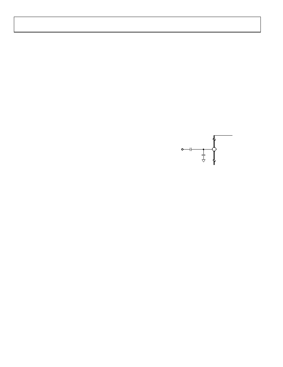
capacitor to ground at the input pin of the IC (Pin 7) to
lower the source impedance at high frequencies, as shown
in Figure 25. A capacitor with a value of 1000 pF is a good
starting value and sets a low-pass corner at 31 kHz for 5 k
sources. In applications where the source ground is not as
clean as would be desirable, a capacitor (illustrated as C7
on the evaluation board) from the VCAR input to the source
ground may prove beneficial. This capacitor is used in
addition to the grounded capacitor (illustrated as C2 on the
evaluation board) used in the feedback around the buffer,
assuming that the buffer is configured for gain.
00357-
024
NOTES
1. ADDITIONAL CIRCUIT DETAILS OMITTED
CX
1000pF
AUDIO +IN
(RS > 5k)
AUDIO +IN
SSM2166
C1
0.1F
7
FOR CLARITY.
Figure 25. Circuit Configuration for Use with High Impedance Signal Sources
The value of C7 should be the same as C6, which is the capacitor
value used between BUF OUT and VCAIN. This connection
makes the source ground noise appear as a common-mode signal
to the VCA, allowing the common-mode noise to be rejected by
the VCA differential input circuitry. C7 can also be useful in
reducing ground loop problems and in reducing noise coupling
from the power supply by balancing the impedances connected
to the inputs of the internal VCA.
相关PDF资料 |
PDF描述 |
|---|---|
| VE-26Z-IU-F4 | CONVERTER MOD DC/DC 2V 80W |
| VE-J5P-MY-B1 | CONVERTER MOD DC/DC 13.8V 50W |
| VI-B1M-IV-F2 | CONVERTER MOD DC/DC 10V 150W |
| MS27473E14B18SLC | CONN HSG PLUG 18POS STRGHT SCKT |
| VE-J5M-MY-B1 | CONVERTER MOD DC/DC 10V 50W |
相关代理商/技术参数 |
参数描述 |
|---|---|
| SSM2166SZ-REEL1 | 制造商:AD 制造商全称:Analog Devices 功能描述:Microphone Preamplifier with Variable Compression and Noise Gating |
| SSM2166SZ-REEL7 | 功能描述:IC PREAMP AUDIO MONO MIC 14SOIC RoHS:是 类别:集成电路 (IC) >> 线性 - 音頻放大器 系列:- 标准包装:80 系列:- 类型:AB 类 输出类型:1-通道(单声道) 在某负载时最大输出功率 x 通道数量:1.25W x 1 @ 8 欧姆 电源电压:2.5 V ~ 5.5 V 特点:消除爆音,差分输入,关闭,热保护 安装类型:表面贴装 供应商设备封装:8-MSOP-PowerPad 封装/外壳:8-TSSOP,8-MSOP(0.118",3.00mm 宽)裸露焊盘 包装:管件 配用:296-31419-ND - EVAL MODULE FOR TPA6205A1 其它名称:296-34563-5TPA6205A1DGN-ND |
| SSM2166SZ-REEL71 | 制造商:AD 制造商全称:Analog Devices 功能描述:Microphone Preamplifier with Variable Compression and Noise Gating |
| SSM2166SZ-X | 制造商:Analog Devices 功能描述:MICROPHONE PREAMPLIFIER W/VAR COMPRESS, ROHS - Rail/Tube |
| SSM2167 | 制造商:AD 制造商全称:Analog Devices 功能描述:Low Voltage Microphone Preamplifier with Variable Compression and Noise Gating |
发布紧急采购,3分钟左右您将得到回复。