- 您现在的位置:买卖IC网 > PDF目录10940 > SSM2603CPZ-REEL (Analog Devices Inc)IC CODEC AUDIO LOW POWER 28LFCSP PDF资料下载
参数资料
| 型号: | SSM2603CPZ-REEL |
| 厂商: | Analog Devices Inc |
| 文件页数: | 3/32页 |
| 文件大小: | 0K |
| 描述: | IC CODEC AUDIO LOW POWER 28LFCSP |
| 标准包装: | 5,000 |
| 类型: | 立体声音频 |
| 分辨率(位): | 24 b |
| ADC / DAC 数量: | 2 / 2 |
| 三角积分调变: | 无 |
| S/N 比,标准 ADC / DAC (db): | 90 / 100 |
| 电压 - 电源,模拟: | 1.8 V ~ 3.6 V |
| 电压 - 电源,数字: | 1.5 V ~ 3.6 V |
| 工作温度: | -40°C ~ 85°C |
| 安装类型: | 表面贴装 |
| 封装/外壳: | 28-VFQFN 裸露焊盘,CSP |
| 供应商设备封装: | 28-LFCSP-VQ |
| 包装: | 带卷 (TR) |
第1页第2页当前第3页第4页第5页第6页第7页第8页第9页第10页第11页第12页第13页第14页第15页第16页第17页第18页第19页第20页第21页第22页第23页第24页第25页第26页第27页第28页第29页第30页第31页第32页
Data Sheet
SSM2603
Rev. C | Page 11 of 32
THEORY OF OPERATION
DIGITAL CORE CLOCK
Inside the SSM2603 digital core is one central clock source, called
the core clock, that produces a reference clock for all internal audio
data processing and synchronization. When using an external
clock source to drive the MCLK pin, great care should be taken
to select a clock source with less than 50 ps of jitter. Without
careful generation of the MCLK signal, the digital audio quality
may suffer.
To enable the SSM2603 to generate the central reference clock in a
system, connect a crystal oscillator between the MCLK/XTI input
pin and the XTO output pin.
To allow an external device to generate the central reference clock,
apply the external clock signal directly through the MCLK/XTI
input pin. In this configuration, the oscillator circuit of the
SSM2603 can be powered down by using the OSC bit (Register R6,
Bit D5) to reduce power consumption.
To accommodate applications with very high frequency master
clocks, the internal core reference clock of the SSM2603 can be
set to either MCLK or MCLK divided by 2. This is enabled by
adjusting the setting of the CLKDIV2 bit (Register R8, Bit D6).
Complementary to this feature, the CLKOUT pin can also drive
external clock sources with either the core clock signal or core
clock divided by 2 by enabling the CLKODIV2 bit (Register R8,
Bit D7).
When activating the digital core of the SSM2603, it is important
for the user to follow this sequence: After activating the desired
power-on blocks from Register R6, some delay time should be
inserted prior to activating the active bit (Register R9, Bit D0),
which enables the digital core.
The delay time is approximated by the following equation:
t = C × 25,000/3.5
where C is the decoupling capacitor on the VMID pin. For
example, if C = 4.7 μF, t = 34 ms.
ADC AND DAC
The SSM2603 contains a pair of oversampling Σ-Δ ADCs. The
maximum ADC full-scale input level is 1.0 V rms when AVDD
= 3.3 V. If the input signal to the ADC exceeds this level, data
overloading occurs and causes audible distortion.
The ADC can accept analog audio input from either the stereo
line inputs or the monaural microphone input. Note that the
ADC can only accept input from a single source, so the user
must choose either the line inputs or the microphone input as
the source using the INSEL bit (Register R4, Bit D2). The digital
data from the ADC output, once converted, is processed using
the ADC filters.
Complementary to the ADC channels, the SSM2603 contains a
pair of oversampling Σ-Δ DACs that convert the digital audio
data from the internal DAC filters into an analog audio signal.
The DAC output can also be muted by setting the DACMU bit
(Register R5, Bit D3) in the control register.
ADC HIGH-PASS AND DAC DE-EMPHASIS FILTERS
The ADC and DAC employ separate digital filters that perform
24-bit signal processing. The digital filters are used for both record
and playback modes and are optimized for each individual
sampling rate used.
For recording mode operations, the unprocessed data from the
ADC enters the ADC filters and is converted to the appropriate
sampling frequency, and then is output to the digital audio
interface.
For playback mode operations, the DAC filters convert the
digital audio interface data to oversampled data, using a sampling
rate selected by the user. The oversampled data is processed by
the DAC and then is sent to the analog output mixer by
enabling the DACSEL (Register R4, Bit D4).
Users have the option of setting up the device so that any dc
offset in the input source signal is automatically detected and
removed. To accomplish this, enable the digital high-pass filter
(see Table 2 for characteristics) contained in the ADC digital
filters by using the ADCHPF bit (Register R5, Bit D0).
In addition, users can implement digital de-emphasis by using
the DEEMPH bits (Register R5, Bit D1 and Bit D2).
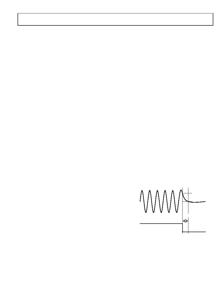
HARDWARE MUTE PIN
MUTE is a hardware mute pin that puts the DAC output of the
SSM2603 codec into a silent state. When MUTE is activated and
the codec enters a mute state, the playback output voltage settles
to VMID. The enabling of MUTE is shown in Figure 17.
Figure 17. Enabling of MUTE
PLAYBACK
OUTPUT
WAVEFORM
MUTE
102,400/MCLK
07
24
1-
01
8
相关PDF资料 |
PDF描述 |
|---|---|
| VI-B21-IW-B1 | CONVERTER MOD DC/DC 12V 100W |
| CS42L55-CNZR | IC CODEC STER H-HDPN AMP 36-QFN |
| DSP56F807VF80 | IC DSP 80MHZ 60K FLASH 160-BGA |
| VI-B20-IW-B1 | CONVERTER MOD DC/DC 5V 100W |
| MC9328MXLCVM15 | IC MCU I.MXL 150MHZ 256-MAPBGA |
相关代理商/技术参数 |
参数描述 |
|---|---|
| SSM2603CPZ-REEL7 | 功能描述:IC CODEC AUDIO LOW POWER 28LFCSP RoHS:是 类别:集成电路 (IC) >> 接口 - 编解码器 系列:- 标准包装:2,500 系列:- 类型:立体声音频 数据接口:串行 分辨率(位):18 b ADC / DAC 数量:2 / 2 三角积分调变:是 S/N 比,标准 ADC / DAC (db):81.5 / 88 动态范围,标准 ADC / DAC (db):82 / 87.5 电压 - 电源,模拟:2.6 V ~ 3.3 V 电压 - 电源,数字:1.7 V ~ 3.3 V 工作温度:-40°C ~ 85°C 安装类型:表面贴装 封装/外壳:48-WFQFN 裸露焊盘 供应商设备封装:48-TQFN-EP(7x7) 包装:带卷 (TR) |
| SSM2603-EVALZ | 功能描述:BOARD EVALUATION FOR SSM2603 RoHS:是 类别:编程器,开发系统 >> 评估演示板和套件 系列:- 标准包装:1 系列:- 主要目的:电信,线路接口单元(LIU) 嵌入式:- 已用 IC / 零件:IDT82V2081 主要属性:T1/J1/E1 LIU 次要属性:- 已供物品:板,电源,线缆,CD 其它名称:82EBV2081 |
| SSM2603GY | 制造商:SSC 制造商全称:Silicon Standard Corp. 功能描述:P-CHANNEL ENHANCEMENT MODE POWER MOSFET |
| SSM2604 | 制造商:AD 制造商全称:Analog Devices 功能描述:Low Power Audio Codec |
| SSM2604CPZ-R2 | 制造商:Rochester Electronics LLC 功能描述: 制造商:Analog Devices 功能描述: |
发布紧急采购,3分钟左右您将得到回复。