- 您现在的位置:买卖IC网 > PDF目录3914 > SST26VF016-80-5C-QAE (Microchip Technology)IC FLSH SER 16MB 80MHZ SPI 8WSON PDF资料下载
参数资料
| 型号: | SST26VF016-80-5C-QAE |
| 厂商: | Microchip Technology |
| 文件页数: | 16/39页 |
| 文件大小: | 0K |
| 描述: | IC FLSH SER 16MB 80MHZ SPI 8WSON |
| 标准包装: | 98 |
| 系列: | SST26 SQI® |
| 格式 - 存储器: | 闪存 |
| 存储器类型: | FLASH |
| 存储容量: | 16M(2M x 8) |
| 速度: | 80MHz |
| 接口: | Serial Quad I/O™(SQI™) |
| 电源电压: | 2.7 V ~ 3.6 V |
| 工作温度: | 0°C ~ 70°C |
| 封装/外壳: | 8-WDFN 裸露焊盘 |
| 供应商设备封装: | 8-WSON |
| 包装: | 管件 |
第1页第2页第3页第4页第5页第6页第7页第8页第9页第10页第11页第12页第13页第14页第15页当前第16页第17页第18页第19页第20页第21页第22页第23页第24页第25页第26页第27页第28页第29页第30页第31页第32页第33页第34页第35页第36页第37页第38页第39页
�� �
�
�Serial� Quad� I/O� (SQI)� Flash� Memory�
�A� Microchip� Technology� Company�
�SST26VF016� /� SST26VF032�
�Data� Sheet�
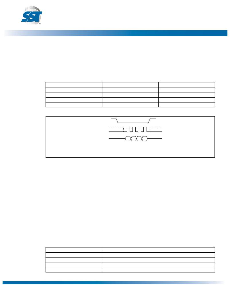
�Set� Burst�
�The� Set� Burst� command� specifies� the� number� of� bytes� to� be� output� during� a� Read� Burst� command�
�before� the� device� wraps� around.� To� set� the� burst� length� the� host� drives� CE#� low,� sends� the� Set� Burst�
�command� cycle� (C0H)� and� one� data� cycle,� then� drives� CE#� high.� A� cycle� is� two� nibbles,� or� two� clocks,�
�long,� most� significant� nibble� first.� After� power-up� or� reset,� the� burst� length� is� set� to� eight� Bytes� (00H).�
�See� Table� 4� for� burst� length� data� and� Figure� 12� for� the� sequence.�
�Table� 4:� Burst� Length� Data�
�Burst� Length�
�8� Bytes�
�16� Bytes�
�32� Bytes�
�64� Bytes�
�High� Nibble� (H0)�
�0h�
�0h�
�0h�
�0h�
�Low� Nibble� (L0)�
�0h�
�1h�
�2h�
�3h�
�T4.0� 25017�
�CE#�
�MODE� 3�
�0�
�1�
�2�
�3�
�SCK�
�SIO(3:0)�
�MODE� 0�
�C1� C0� H0� L0�
�MSN� LSN�
�1359� F32.0�
�Note:� MSN� =� Most� Significant� Nibble,�
�LSN� =� Least� Significant� Nibble�
�Figure� 12:� Set� Burst� Length� Sequence�
�Read� Burst�
�To� execute� a� Read� Burst� operation� the� host� drives� CE#� low,� then� sends� the� Read� Burst� command�
�cycle� (0CH),� followed� by� three� address� cycles,� and� then� one� dummy� cycle.� Each� cycle� is� two� nibbles�
�(clocks)� long,� most� significant� nibble� first.�
�After� the� dummy� cycle,� the� device� outputs� data� on� the� falling� edge� of� the� SCK� signal� starting� from� the�
�specified� address� location.� The� data� output� stream� is� continuous� through� all� addresses� until� termi-�
�nated� by� a� low-to-high� transition� on� CE#.�
�During� Read� Burst,� the� internal� address� pointer� automatically� increments� until� the� last� byte� of� the� burst�
�is� reached,� then� jumps� to� first� byte� of� the� burst.� All� bursts� are� aligned� to� addresses� within� the� burst�
�length,� see� Table� 5.� For� example,� if� the� burst� length� is� eight� Bytes,� and� the� start� address� is� 06h,� the�
�burst� sequence� would� be:� 06h,� 07h,� 00h,� 01h,� 02h,� 03h,� 04h,� 05h,� 06h,� etc.� The� pattern� would� repeat�
�until� the� command� was� terminated� by� a� low-to-high� transition� on� CE#.�
�During� this� operation,� blocks� that� are� Read-locked� will� output� data� 00H.�
�Table� 5:� Burst� Address� Ranges�
�Burst� Length�
�8� Bytes�
�16� Bytes�
�32� Bytes�
�64� Bytes�
�Burst� Address� Ranges�
�00-07H,� 08-0FH,� 10-17H,� 18-1FH...�
�00-0FH,� 10-1FH,� 20-2FH,� 30-3FH...�
�00-1FH,� 20-3FH,� 40-5FH,� 60-7FH...�
�00-3FH,� 40-7FH,� 80-BFH,� C0-FFH�
�T5.0� 25017�
�?2011� Silicon� Storage� Technology,� Inc.�
�16�
�DS-25017A�
�04/11�
�相关PDF资料 |
PDF描述 |
|---|---|
| SST39WF800A-90-4C-B3KE | IC FLASH MPF 8MBIT 90NS 48TFBGA |
| MM908E621ACDWB | IC QUAD HALF BRDG TRPL SW 54SOIC |
| MM908E624ACDWB | IC TRPL SWITCH MCU/LIN 54-SOIC |
| MM908E624ACDWBR2 | IC TRPL SWITCH MCU/LIN 54-SOIC |
| 046232108015800+ | CONN FFC/FPC 8POS 1MM VERT SMD |
相关代理商/技术参数 |
参数描述 |
|---|---|
| SST26VF016-80-5C-S2AE | 功能描述:闪存 2.7 to 3.6V 16Mbit Serial Quad I/O Flsh RoHS:否 制造商:ON Semiconductor 数据总线宽度:1 bit 存储类型:Flash 存储容量:2 MB 结构:256 K x 8 定时类型: 接口类型:SPI 访问时间: 电源电压-最大:3.6 V 电源电压-最小:2.3 V 最大工作电流:15 mA 工作温度:- 40 C to + 85 C 安装风格:SMD/SMT 封装 / 箱体: 封装:Reel |
| SST26VF016-80-5I-QAE | 功能描述:闪存 16M 80MHz 2.7-3.6V Industrial RoHS:否 制造商:ON Semiconductor 数据总线宽度:1 bit 存储类型:Flash 存储容量:2 MB 结构:256 K x 8 定时类型: 接口类型:SPI 访问时间: 电源电压-最大:3.6 V 电源电压-最小:2.3 V 最大工作电流:15 mA 工作温度:- 40 C to + 85 C 安装风格:SMD/SMT 封装 / 箱体: 封装:Reel |
| SST26VF016-80-5I-QAE-T | 功能描述:闪存 2.7 to 3.6V 16Mbit Serial Quad I/O Flsh RoHS:否 制造商:ON Semiconductor 数据总线宽度:1 bit 存储类型:Flash 存储容量:2 MB 结构:256 K x 8 定时类型: 接口类型:SPI 访问时间: 电源电压-最大:3.6 V 电源电压-最小:2.3 V 最大工作电流:15 mA 工作温度:- 40 C to + 85 C 安装风格:SMD/SMT 封装 / 箱体: 封装:Reel |
| SST26VF016-80-5I-QE | 制造商:SST 制造商全称:Silicon Storage Technology, Inc 功能描述:Serial Quad I/O (SQI) Flash Memory |
| SST26VF016-80-5I-S2AE | 功能描述:闪存 16M 80MHz 2.7-3.6V Industrial RoHS:否 制造商:ON Semiconductor 数据总线宽度:1 bit 存储类型:Flash 存储容量:2 MB 结构:256 K x 8 定时类型: 接口类型:SPI 访问时间: 电源电压-最大:3.6 V 电源电压-最小:2.3 V 最大工作电流:15 mA 工作温度:- 40 C to + 85 C 安装风格:SMD/SMT 封装 / 箱体: 封装:Reel |
发布紧急采购,3分钟左右您将得到回复。