- 您现在的位置:买卖IC网 > PDF目录4544 > SST39VF3202B-70-4I-EKE (Microchip Technology)IC FLASH MPF 32MBIT 70NS 48TSOP PDF资料下载
参数资料
| 型号: | SST39VF3202B-70-4I-EKE |
| 厂商: | Microchip Technology |
| 文件页数: | 3/29页 |
| 文件大小: | 0K |
| 描述: | IC FLASH MPF 32MBIT 70NS 48TSOP |
| 特色产品: | SST Serial and Parallel Flash Memory |
| 标准包装: | 96 |
| 系列: | SST39 MPF™ |
| 格式 - 存储器: | 闪存 |
| 存储器类型: | FLASH |
| 存储容量: | 32M(2M x 16) |
| 速度: | 70ns |
| 接口: | 并联 |
| 电源电压: | 2.7 V ~ 3.6 V |
| 工作温度: | -40°C ~ 85°C |
| 封装/外壳: | 48-TFSOP(0.724",18.40mm 宽) |
| 供应商设备封装: | 48-TSOP |
| 包装: | 管件 |
第1页第2页当前第3页第4页第5页第6页第7页第8页第9页第10页第11页第12页第13页第14页第15页第16页第17页第18页第19页第20页第21页第22页第23页第24页第25页第26页第27页第28页第29页
�� �
�
�32� Mbit� Multi-Purpose� Flash� Plus�
�SST39VF3201B� /� SST39VF3202B�
�Data� Sheet�
�Chip-Erase� Operation�
�The� SST39VF320xB� provide� a� Chip-Erase� operation,�
�which� allows� the� user� to� erase� the� entire� memory� array� to�
�the� “1”� state.� This� is� useful� when� the� entire� device� must� be�
�quickly� erased.�
�The� Chip-Erase� operation� is� initiated� by� executing� a� six-�
�byte� command� sequence� with� Chip-Erase� command�
�(10H)� at� address� 555H� in� the� last� byte� sequence.� The�
�Erase� operation� begins� with� the� rising� edge� of� the� sixth�
�WE#� or� CE#,� whichever� occurs� first.� During� the� Erase�
�operation,� the� only� valid� read� is� Toggle� Bit� or� Data#� Polling.�
�See� Table� 6� for� the� command� sequence,� Figure� 10� for� tim-�
�ing� diagram,� and� Figure� 25� for� the� flowchart.� Any� com-�
�mands� issued� during� the� Chip-Erase� operation� are�
�ignored.� When� WP#� is� low,� any� attempt� to� Chip-Erase� will�
�be� ignored.� During� the� command� sequence,� WP#� should�
�be� statically� held� high� or� low.�
�Write� Operation� Status� Detection�
�The� SST39VF320xB� provide� two� software� means� to� detect�
�the� completion� of� a� Write� (Program� or� Erase)� cycle,� in�
�order� to� optimize� the� system� write� cycle� time.� The� software�
�detection� includes� two� status� bits:� Data#� Polling� (DQ� 7� )� and�
�Toggle� Bit� (DQ� 6� ).� The� End-of-Write� detection� mode� is�
�enabled� after� the� rising� edge� of� WE#,� which� initiates� the�
�internal� Program� or� Erase� operation.�
�The� actual� completion� of� the� nonvolatile� write� is� asyn-�
�chronous� with� the� system;� therefore,� either� a� Data#� Poll-�
�‘1’.� The� Data#� Polling� is� valid� after� the� rising� edge� of� fourth�
�WE#� (or� CE#)� pulse� for� Program� operation.� For� Sector-,�
�Block-� or� Chip-Erase,� the� Data#� Polling� is� valid� after� the�
�rising� edge� of� sixth� WE#� (or� CE#)� pulse.� See� Figure� 8� for�
�Data#� Polling� timing� diagram� and� Figure� 22� for� a� flowchart.�
�Toggle� Bits� (DQ6� and� DQ2)�
�During� the� internal� Program� or� Erase� operation,� any� con-�
�secutive� attempts� to� read� DQ� 6� will� produce� alternating� “1”s�
�and� “0”s,� i.e.,� toggling� between� 1� and� 0.� When� the� internal�
�Program� or� Erase� operation� is� completed,� the� DQ� 6� bit� will�
�stop� toggling.� The� device� is� then� ready� for� the� next� opera-�
�tion.� For� Sector-,� Block-,� or� Chip-Erase,� the� toggle� bit� (DQ� 6� )�
�is� valid� after� the� rising� edge� of� sixth� WE#� (or� CE#)� pulse.�
�DQ� 6� will� be� set� to� ‘1’� if� a� Read� operation� is� attempted� on� an�
�Erase-Suspended� Sector/Block.� If� Program� operation� is� ini-�
�tiated� in� a� sector/block� not� selected� in� Erase-Suspend�
�mode,� DQ� 6� will� toggle.�
�An� additional� Toggle� Bit� is� available� on� DQ� 2� ,� which� can� be�
�used� in� conjunction� with� DQ� 6� to� check� whether� a� particular�
�sector� is� being� actively� erased� or� erase-suspended.� Table� 1�
�shows� detailed� status� bits� information.� The� Toggle� Bit�
�(DQ� 2� )� is� valid� after� the� rising� edge� of� the� last� WE#� (or� CE#)�
�pulse� of� Write� operation.� See� Figure� 9� for� Toggle� Bit� timing�
�diagram� and� Figure� 22� for� a� flowchart.�
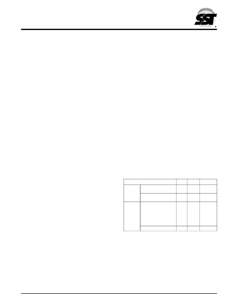
�TABLE� 1:� Write� Operation� Status�
�ing� or� Toggle� Bit� read� may� be� simultaneous� with� the�
�Status�
�DQ� 7�
�DQ� 6�
�DQ� 2�
�completion� of� the� write� cycle.� If� this� occurs,� the� system�
�Normal�
�Standard�
�DQ� 7� #�
�Toggle�
�No� Toggle�
�may� possibly� get� an� erroneous� result,� i.e.,� valid� data� may�
�Operation� Program�
�appear� to� conflict� with� either� DQ� 7� or� DQ� 6� .� In� order� to� pre-�
�vent� spurious� rejection,� if� an� erroneous� result� occurs,� the�
�Standard�
�Erase�
�0�
�Toggle�
�Toggle�
�software� routine� should� include� a� loop� to� read� the�
�accessed� location� an� additional� two� (2)� times.� If� both�
�reads� are� valid,� then� the� device� has� completed� the� Write�
�cycle,� otherwise� the� rejection� is� valid.�
�Erase-�
�Suspend�
�Mode�
�Read� from�
�Erase-Suspended�
�Sector/Block�
�Read� from�
�Non-� Erase-Suspended�
�1�
�Data�
�1�
�Data�
�Toggle�
�Data�
�Sector/Block�
�Data#� Polling� (DQ� 7� )�
�Program�
�DQ� 7� #�
�Toggle�
�N/A�
�T1.0� 1384�
�When� the� SST39VF320xB� are� in� the� internal� Program�
�operation,� any� attempt� to� read� DQ� 7� will� produce� the� com-�
�plement� of� the� true� data.� Once� the� Program� operation� is�
�completed,� DQ� 7� will� produce� true� data.� Note� that� even�
�though� DQ� 7� may� have� valid� data� immediately� following� the�
�completion� of� an� internal� Write� operation,� the� remaining�
�data� outputs� may� still� be� invalid:� valid� data� on� the� entire�
�data� bus� will� appear� in� subsequent� successive� Read�
�cycles� after� an� interval� of� 1� μs.� During� internal� Erase� oper-�
�ation,� any� attempt� to� read� DQ� 7� will� produce� a� ‘0’.� Once� the�
�internal� Erase� operation� is� completed,� DQ� 7� will� produce� a�
�Note:� DQ� 7� ,� DQ� 6� and� DQ� 2� require� a� valid� address� when� reading�
�status� information.�
�?2009� Silicon� Storage� Technology,� Inc.�
�3�
�S71384-01-000�
�1/09�
�相关PDF资料 |
PDF描述 |
|---|---|
| HSM44DRTF-S13 | CONN EDGECARD 88POS .156 EXTEND |
| HMM44DRTF-S13 | CONN EDGECARD 88POS .156 EXTEND |
| RSM40DRMD | CONN EDGECARD 80POS .156 WW |
| RSA43DTMI | CONN EDGECARD 86POS R/A .125 SLD |
| RMA43DTMI | CONN EDGECARD 86POS R/A .125 SLD |
相关代理商/技术参数 |
参数描述 |
|---|---|
| SST39VF3202C-70-4I-B3KE | 功能描述:闪存 2.7V to 3.6V 32Mbit Multi-Prps Fl RoHS:否 制造商:ON Semiconductor 数据总线宽度:1 bit 存储类型:Flash 存储容量:2 MB 结构:256 K x 8 定时类型: 接口类型:SPI 访问时间: 电源电压-最大:3.6 V 电源电压-最小:2.3 V 最大工作电流:15 mA 工作温度:- 40 C to + 85 C 安装风格:SMD/SMT 封装 / 箱体: 封装:Reel |
| SST39VF3202C-70-4I-B3KE-T | 功能描述:闪存 2.7V to 3.6V 32Mbit Multi-Prps Fl RoHS:否 制造商:ON Semiconductor 数据总线宽度:1 bit 存储类型:Flash 存储容量:2 MB 结构:256 K x 8 定时类型: 接口类型:SPI 访问时间: 电源电压-最大:3.6 V 电源电压-最小:2.3 V 最大工作电流:15 mA 工作温度:- 40 C to + 85 C 安装风格:SMD/SMT 封装 / 箱体: 封装:Reel |
| SST39VF3202C-70-4I-EKE | 功能描述:闪存 2.7V to 3.6V 32Mbit Multi-Prps Fl RoHS:否 制造商:ON Semiconductor 数据总线宽度:1 bit 存储类型:Flash 存储容量:2 MB 结构:256 K x 8 定时类型: 接口类型:SPI 访问时间: 电源电压-最大:3.6 V 电源电压-最小:2.3 V 最大工作电流:15 mA 工作温度:- 40 C to + 85 C 安装风格:SMD/SMT 封装 / 箱体: 封装:Reel |
| SST39VF3202C-70-4I-EKE-T | 功能描述:闪存 2.7V to 3.6V 32Mbit Multi-Prps Fl RoHS:否 制造商:ON Semiconductor 数据总线宽度:1 bit 存储类型:Flash 存储容量:2 MB 结构:256 K x 8 定时类型: 接口类型:SPI 访问时间: 电源电压-最大:3.6 V 电源电压-最小:2.3 V 最大工作电流:15 mA 工作温度:- 40 C to + 85 C 安装风格:SMD/SMT 封装 / 箱体: 封装:Reel |
| SST39VF320-70-4C-B3K | 功能描述:闪存 2M X 16 70ns RoHS:否 制造商:ON Semiconductor 数据总线宽度:1 bit 存储类型:Flash 存储容量:2 MB 结构:256 K x 8 定时类型: 接口类型:SPI 访问时间: 电源电压-最大:3.6 V 电源电压-最小:2.3 V 最大工作电流:15 mA 工作温度:- 40 C to + 85 C 安装风格:SMD/SMT 封装 / 箱体: 封装:Reel |
发布紧急采购,3分钟左右您将得到回复。