- 您现在的位置:买卖IC网 > PDF目录384931 > ST16C2550IQ48 (EXAR CORP) DUAL UART WITH 16-BYTE TRANSMIT AND RECEIVE FIFO’S PDF资料下载
参数资料
| 型号: | ST16C2550IQ48 |
| 厂商: | EXAR CORP |
| 元件分类: | 微控制器/微处理器 |
| 英文描述: | DUAL UART WITH 16-BYTE TRANSMIT AND RECEIVE FIFO’S |
| 中文描述: | 2 CHANNEL(S), 4M bps, SERIAL COMM CONTROLLER, PQFP48 |
| 封装: | 7 X 7 MM, 1 MM HEIGHT, TQFP-48 |
| 文件页数: | 10/34页 |
| 文件大小: | 443K |
| 代理商: | ST16C2550IQ48 |
第1页第2页第3页第4页第5页第6页第7页第8页第9页当前第10页第11页第12页第13页第14页第15页第16页第17页第18页第19页第20页第21页第22页第23页第24页第25页第26页第27页第28页第29页第30页第31页第32页第33页第34页
ST16C2550
10
Rev. 3.20
ing the removal of a data byte, the user should recheck
LSR bit-0 for additional characters. A Receive Time
Out will not occur if the receive FIFO is empty. The
time out counter is reset at the center of each stop bit
received or each time the receive holding register
(RHR) is read.. The actual time out value is T (
T
ime
out length in bits) = 4 X P (
P
rogrammed word length)
+ 12. To convert the time out value to a character
value, the user has to consider the complete word
length, including data information length, start bit,
parity bit, and the size of stop bit, i.e., 1X, 1.5X, or 2X
bit times.
Example -A: If the user programs a word length of 7,
with no parity and one stop bit, the time out will be:
T = 4 X 7( programmed word length) +12 = 40 bit times.
The character time will be equal to 40 / 9 = 4.4
characters, or as shown in the fully worked out ex-
ample: T = [(programmed word length = 7) + (stop bit
= 1) + (start bit = 1) = 9]. 40 (bit times divided by 9) =
4.4 characters.
Example -B: If the user programs the word length = 7,
with parity and one stop bit, the time out will be:
T = 4 X 7(programmed word length) + 12 = 40 bit times.
Character time = 40 / 10 [ (programmed word length
= 7) + (parity = 1) + (stop bit = 1) + (start bit = 1) = 4
characters.
Programmable Baud Rate Generator
The 2550 supports high speed modem technologies
that have increased input data rates by employing
data compression schemes. For example a 33.6Kbps
modem that employs data compression may require a
115.2Kbps input data rate. A 128.0Kbps ISDN modem
that supports data compression may need an input
data rate of 460.8Kbps. The 2550 can support a
standard data rate of 921.6Kbps.
Single baud rate generator is provided for the trans-
mitter and receiver, allowing independent TX/RX
channel control. The programmable Baud Rate Gen-
erator is capable of accepting an input clock up to 24
MHz, as required for supporting a 1.5Mbps data rate.
The 2550 can be configured for internal or external
clock operation. For internal clock oscillator opera-
tion, an industry standard microprocessor crystal (par-
allel resonant/ 22-33 pF load) is connected externally
between the XTAL1 and XTAL2 pins, with an external
1 M
resistor across it. Alternatively, an external
clock can be connected to the XTAL1 pin to clock the
internal baud rate generator for standard or custom
rates. (see Baud Rate Generator Programming).
The generator divides the input 16X clock by any
divisor from 1 to 2
16
-1. The 2550 divides the basic
external clock by 16. The basic 16X clock provides
table rates to support standard and custom applica-
tions using the same system design. The rate table is
configured via the DLL and DLM internal register
functions. Customized Baud Rates can be achieved
by selecting the proper divisor values for the MSB and
LSB sections of baud rate generator.
Programming the Baud Rate Generator Registers
DLM (MSB) and DLL (LSB) provides a user capability
for selecting the desired final baud rate. The example
in Table 4 below, shows the selectable baud rate table
available when using a 1.8432 MHz external clock
input.
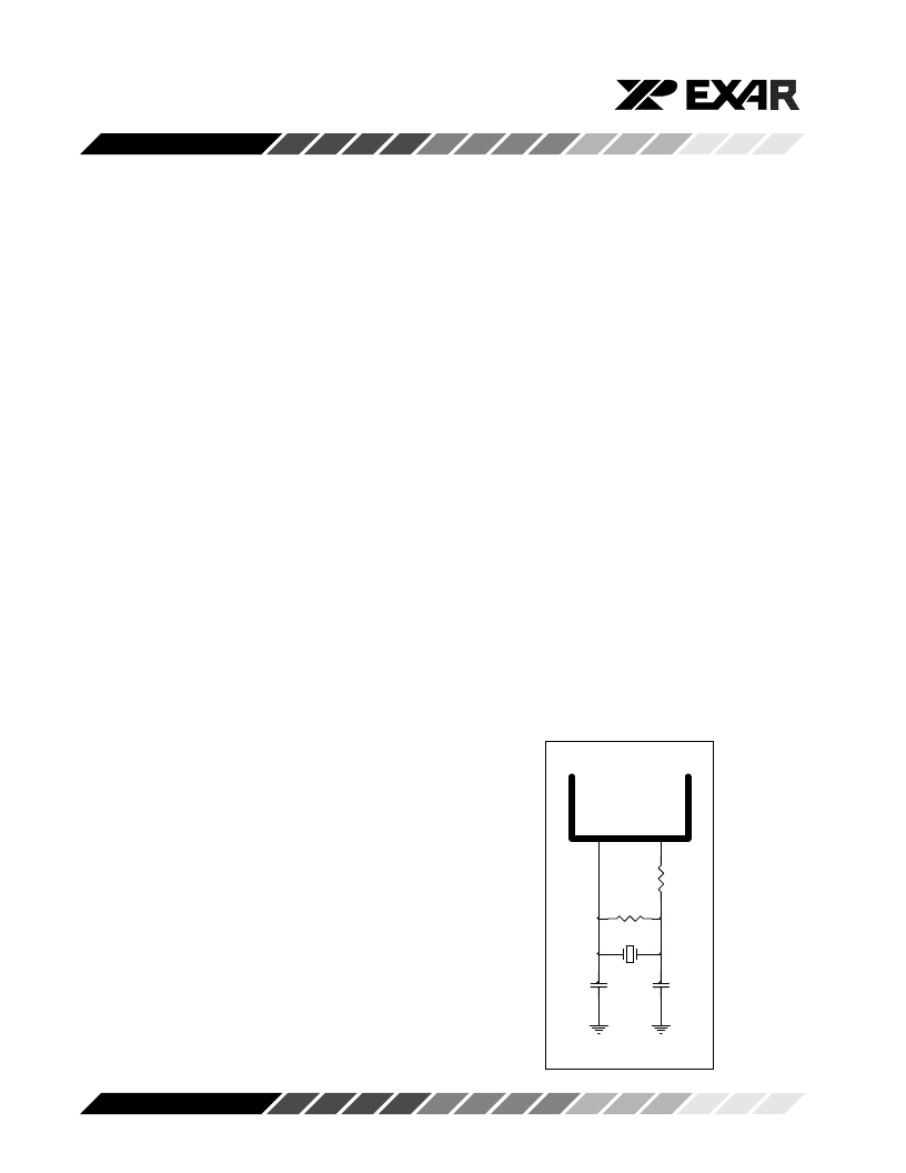
Crystal oscillator connection
C1
22pF
C2
33pF
X1
1.8432 MHz
R1
50-120
R2
1M
X
X
相关PDF资料 |
PDF描述 |
|---|---|
| ST16C2550 | Dual UART with 16-Byte of Transmit and Receive FIFO(双通用异步接收器/发送器(带16字节接收和发送先进先出)) |
| ST16C2552 | Dual UART with 16-Byte Transmit and Receive FIFO(双通用异步接收器/发送器(带16字节接收和发送先进先出)) |
| ST16C450 | UNIVERSAL ASYNCHRONOUS RECEIVER/TRANSMITTER (UART) |
| ST16C450CJ44 | UNIVERSAL ASYNCHRONOUS RECEIVER/TRANSMITTER (UART) |
| ST16C450CP40 | UNIVERSAL ASYNCHRONOUS RECEIVER/TRANSMITTER (UART) |
相关代理商/技术参数 |
参数描述 |
|---|---|
| ST16C2550IQ48-F | 功能描述:UART 接口集成电路 2.97V-5.5V 16B FIFO temp -45 to 85C;UART RoHS:否 制造商:Texas Instruments 通道数量:2 数据速率:3 Mbps 电源电压-最大:3.6 V 电源电压-最小:2.7 V 电源电流:20 mA 最大工作温度:+ 85 C 最小工作温度:- 40 C 封装 / 箱体:LQFP-48 封装:Reel |
| ST16C2550IQ48TR-F | 功能描述:UART 接口集成电路 DUAL UART W/16BYTE FIFO RoHS:否 制造商:Texas Instruments 通道数量:2 数据速率:3 Mbps 电源电压-最大:3.6 V 电源电压-最小:2.7 V 电源电流:20 mA 最大工作温度:+ 85 C 最小工作温度:- 40 C 封装 / 箱体:LQFP-48 封装:Reel |
| ST16C2552 | 制造商:EXAR 制造商全称:EXAR 功能描述:2.97V TO 5.5V DUAL UART WITH 16-BYTE FIFO |
| ST16C2552_06 | 制造商:EXAR 制造商全称:EXAR 功能描述:2.97V TO 5.5V DUAL UART WITH 16-BYTE FIFO |
| ST16C2552CJ | 制造商:EXAR 功能描述:IC , Dual UART 4MBPS 5.5 44 PLCC 制造商:Exar Corporation 功能描述: 制造商:XIC 功能描述: 制造商:Exar Corporation 功能描述:UART, 44 Pin, Plastic, PLCC |
发布紧急采购,3分钟左右您将得到回复。