- 您现在的位置:买卖IC网 > PDF目录299933 > ST24C04R (意法半导体) Serial 4K (512 x 8) EEPROM(串行4K EEPROM) PDF资料下载
参数资料
| 型号: | ST24C04R |
| 厂商: | 意法半导体 |
| 英文描述: | Serial 4K (512 x 8) EEPROM(串行4K EEPROM) |
| 中文描述: | 串行4K的(512 × 8)的EEPROM(4K的串行EEPROM中) |
| 文件页数: | 2/16页 |
| 文件大小: | 163K |
| 代理商: | ST24C04R |
The sequence is as follows:
– Initial condition: a Write is in progress (see Figure
8).
– Step 1: the Master issues a START condition
followed by a Device Select byte (1st byte of the
new instruction).
– Step 2: if the memory is busy with the internal
write cycle, no ACK will be returned and the
master goes back to Step 1. If the memory has
terminated the internal write cycle, it will
re-
spond with an ACK, indicating that the memory
is ready to receive the second part of the next
instruction (the first byte of this instruction was
already sent during Step 1).
Write Protection. Data in the upper block of 256
bytes of the memory may be write protected. The
memory is write protected between a boundary
address and the top of memory (address 1FFh)
when the PRE input pin is taken high and when the
Protect Flag (bit b2 in location 1FFh) is set to ’0’.
The boundary address is user defined by writing it
in the Block Address Pointer. The Block Address
Pointer is an 8 bit EEPROM register located at the
address 1FFh. It is composed by 5 MSBs Address
Pointer, which defines the bottom boundary ad-
dress, and 3 LSBs which must be programmed at
DEVICE OPERATION (cont’d)
’0’. This Address Pointer can therefore address a
boundary in steps of 8 bytes.
The sequence to use the Write Protected feature
is:
– write the data to be protected into the top of the
memory, up to, but not including, location 1FFh;
– set the protection by writing the correct bottom
boundary address in the
Address Pointer (5
MSBs of location 1FFh) with bit b2 (Protect flag)
set to ’0’. Note that for a correct fonctionality of
the memory, all the 3 LSBs of the Block Address
Pointer must also be programmed at ’0’.
The area will now be protected when the PRE input
pin is taken High. While the PRE input pin is read
at ’0’ by the memory, the location 1FFh can be used
as a normal EEPROM byte.
Caution: Special attention must be used when
using the protect mode together with the Multibyte
Write mode (MODE input pin High). If the Multibyte
Write starts at the location right below the first byte
of the Write Protected area, then the instruction will
write over the first 3 bytes of the Write Protected
area. The area protected is therefore smaller than
the content defined in the location 1FFh, by 3 bytes.
This does not apply to the Page Write mode as the
address counter ’roll-over’ and thus cannot go
above the 8 bytes lower boundary of the protected
area.
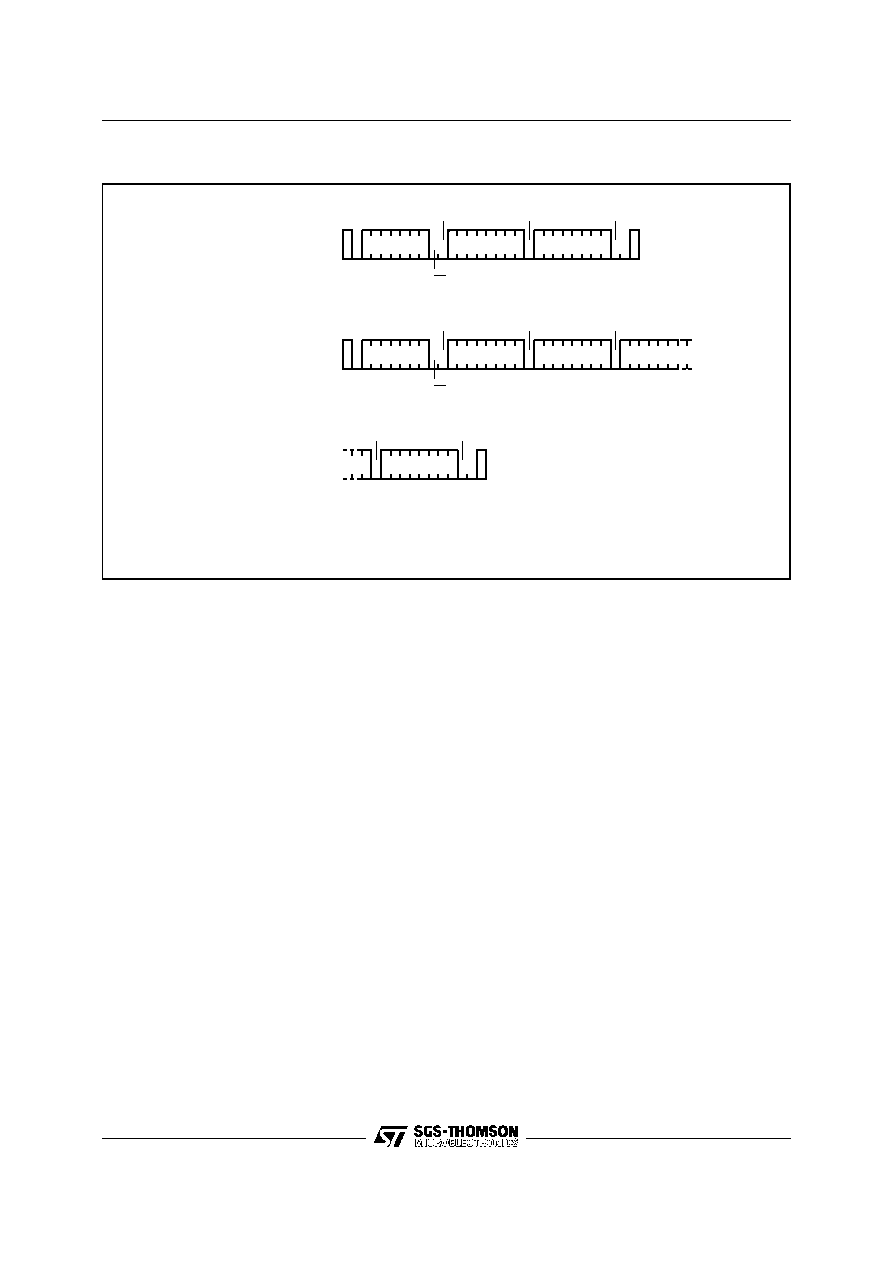
STOP
START
BYTE WRITE
DEV SEL
BYTE ADDR
DATA IN
START
MULTIBYTE
AND
PAGE WRITE
DEV SEL
BYTE ADDR
DATA IN 1
DATA IN 2
AI00793
STOP
DATA IN N
ACK
R/W
ACK
R/W
ACK
Figure 9. Write Modes Sequence (ST24/25C04 and ST24C04R)
10/16
ST24/25C04, ST24C04R, ST24/25W04
相关PDF资料 |
PDF描述 |
|---|---|
| ST25C08M1 | 1K X 8 SPI BUS SERIAL EEPROM, PDSO8 |
| ST280C04C1L | 960 A, 400 V, SCR, TO-200AB |
| ST280C04C2L | 960 A, 400 V, SCR, TO-200AB |
| ST280C04C2 | 960 A, 400 V, SCR, TO-200AB |
| ST280C04C3L | 960 A, 400 V, SCR, TO-200AB |
相关代理商/技术参数 |
参数描述 |
|---|---|
| ST24C04RB1 | 制造商:未知厂家 制造商全称:未知厂家 功能描述:I2C Serial EEPROM |
| ST24C04RB3 | 制造商:未知厂家 制造商全称:未知厂家 功能描述:I2C Serial EEPROM |
| ST24C04RB5 | 制造商:未知厂家 制造商全称:未知厂家 功能描述:I2C Serial EEPROM |
| ST24C04RB6 | 制造商:未知厂家 制造商全称:未知厂家 功能描述:I2C Serial EEPROM |
| ST24C04RM1 | 制造商:未知厂家 制造商全称:未知厂家 功能描述:I2C Serial EEPROM |
发布紧急采购,3分钟左右您将得到回复。