- 您现在的位置:买卖IC网 > PDF目录69350 > ST62P00CB3/XXX (STMICROELECTRONICS) 8-BIT, MROM, 8 MHz, MICROCONTROLLER, PDIP16 PDF资料下载
参数资料
| 型号: | ST62P00CB3/XXX |
| 厂商: | STMICROELECTRONICS |
| 元件分类: | 微控制器/微处理器 |
| 英文描述: | 8-BIT, MROM, 8 MHz, MICROCONTROLLER, PDIP16 |
| 封装: | 0.300 INCH, PLASTIC, DIP-16 |
| 文件页数: | 76/100页 |
| 文件大小: | 1713K |
| 代理商: | ST62P00CB3/XXX |
第1页第2页第3页第4页第5页第6页第7页第8页第9页第10页第11页第12页第13页第14页第15页第16页第17页第18页第19页第20页第21页第22页第23页第24页第25页第26页第27页第28页第29页第30页第31页第32页第33页第34页第35页第36页第37页第38页第39页第40页第41页第42页第43页第44页第45页第46页第47页第48页第49页第50页第51页第52页第53页第54页第55页第56页第57页第58页第59页第60页第61页第62页第63页第64页第65页第66页第67页第68页第69页第70页第71页第72页第73页第74页第75页当前第76页第77页第78页第79页第80页第81页第82页第83页第84页第85页第86页第87页第88页第89页第90页第91页第92页第93页第94页第95页第96页第97页第98页第99页第100页
ST6200C ST6201C ST6203C
77/100
10.8 I/O PORT PIN CHARACTERISTICS
10.8.1 General Characteristics
Subject to general operating conditions for VDD, fOSC, and TA unless otherwise specified.
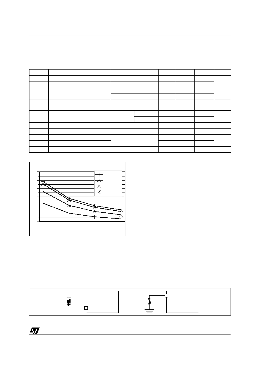
Figure 55. Typical RPU vs. VDD with VIN = VSS
Notes:
1. Unless otherwise specified, typical data are based on TA=25°C and VDD=5V.
2. Data based on characterization results, not tested in production.
3. Hysteresis voltage between Schmitt trigger switching levels. Based on characterization results, not tested.
4. The RPU pull-up equivalent resistor is based on a resistive transistor. This data is based on characterization results,
not tested in production.
5. Data based on characterization results, not tested in production.
6. To generate an external interrupt, a minimum pulse width has to be applied on an I/O port pin configured as an external
interrupt source.
Figure 56. Two typical Applications with unused I/O Pin
Symbol
Parameter
Conditions
Min
Typ 1)
Max
Unit
VIL
Input low level voltage 2)
0.3xVDD
V
VIH
Input high level voltage 2)
0.7xVDD
Vhys
Schmitt trigger voltage hysteresis 3)
VDD=5V
200
400
mV
VDD=3.3V
200
400
IL
Input leakage current
VSS≤VIN≤VDD
(no pull-up configured)
0.1
1
μA
RPU
Weak pull-up equivalent resistor 4)
VIN=VSS
VDD=5V
40
110
350
k
Ω
VDD=3.3V
80
230
700
CIN
I/O input pin capacitance
5
10
pF
COUT
I/O output pin capacitance
5
10
pF
tf(IO)out
Output high to low level fall time 5)
CL=50pF
Between 10% and 90%
30
ns
tr(IO)out
Output low to high level rise time 5)
35
tw(IT)in
External interrupt pulse time 6)
1tCPU
34
56
VDD [V]
50
100
150
200
250
300
350
Rpu [Khom]
Ta=-40°C
Ta=25°C
Ta=95°C
Ta=125°C
10k
Ω
UNUSED I/O PORT
ST62XX
10k
Ω
UNUSED I/O PORT
ST62XX
VDD
1
相关PDF资料 |
PDF描述 |
|---|---|
| ST62T00CM6 | 8-BIT, OTPROM, 8 MHz, MICROCONTROLLER, PDSO16 |
| ST62T00CM1 | 8-BIT, OTPROM, 8 MHz, MICROCONTROLLER, PDSO16 |
| ST62T00CN1 | 8-BIT, OTPROM, 8 MHz, MICROCONTROLLER, PDSO16 |
| ST62T00CN6 | 8-BIT, OTPROM, 8 MHz, MICROCONTROLLER, PDSO16 |
| ST62T01CB3 | 8-BIT, OTPROM, 8 MHz, MICROCONTROLLER, PDIP16 |
相关代理商/技术参数 |
参数描述 |
|---|---|
| ST62P03CM1/MAM | 制造商:STMicroelectronics 功能描述: |
| ST62P08CM6/MHH/TR | 制造商:STMicroelectronics 功能描述: |
| ST62P08CM6/RCFTR | 制造商:STMicroelectronics 功能描述: |
| ST62P09CM1/REXTR | 制造商:STMicroelectronics 功能描述: |
| ST62P10CM6/FBS | 制造商:STMicroelectronics 功能描述: |
发布紧急采购,3分钟左右您将得到回复。