- 您现在的位置:买卖IC网 > PDF目录69350 > ST62P09CB6/XXX (STMICROELECTRONICS) 8-BIT, MROM, 8 MHz, MICROCONTROLLER, PDIP20 PDF资料下载
参数资料
| 型号: | ST62P09CB6/XXX |
| 厂商: | STMICROELECTRONICS |
| 元件分类: | 微控制器/微处理器 |
| 英文描述: | 8-BIT, MROM, 8 MHz, MICROCONTROLLER, PDIP20 |
| 封装: | 0.300 INCH, PLASTIC, DIP-20 |
| 文件页数: | 89/104页 |
| 文件大小: | 1487K |
| 代理商: | ST62P09CB6/XXX |
第1页第2页第3页第4页第5页第6页第7页第8页第9页第10页第11页第12页第13页第14页第15页第16页第17页第18页第19页第20页第21页第22页第23页第24页第25页第26页第27页第28页第29页第30页第31页第32页第33页第34页第35页第36页第37页第38页第39页第40页第41页第42页第43页第44页第45页第46页第47页第48页第49页第50页第51页第52页第53页第54页第55页第56页第57页第58页第59页第60页第61页第62页第63页第64页第65页第66页第67页第68页第69页第70页第71页第72页第73页第74页第75页第76页第77页第78页第79页第80页第81页第82页第83页第84页第85页第86页第87页第88页当前第89页第90页第91页第92页第93页第94页第95页第96页第97页第98页第99页第100页第101页第102页第103页第104页
ST6208C/ST6209C/ST6210C/ST6220C
85/104
10.9 CONTROL PIN CHARACTERISTICS
10.9.1 Asynchronous RESET Pin
Subject to general operating conditions for VDD, fOSC, and TA unless otherwise specified.
Notes:
1. Unless otherwise specified, typical data are based on TA=25°C and VDD=5V.
2. Data based on characterization results, not tested in production.
3. Hysteresis voltage between Schmitt trigger switching levels. Based on characterization results, not tested.
4. The RON pull-up equivalent resistor is based on a resistive transistor. This data is based on characterization results,
not tested in production.
5. All short pulse applied on RESET pin with a duration below th(RSTL)in can be ignored.
6. The reset network protects the device against parasitic resets, especially in a noisy environment.
7. The output of the external reset circuit must have an open-drain output to drive the ST6 reset pad. Otherwise the device
can be damaged when the ST6 generates an internal reset (LVD or watchdog).
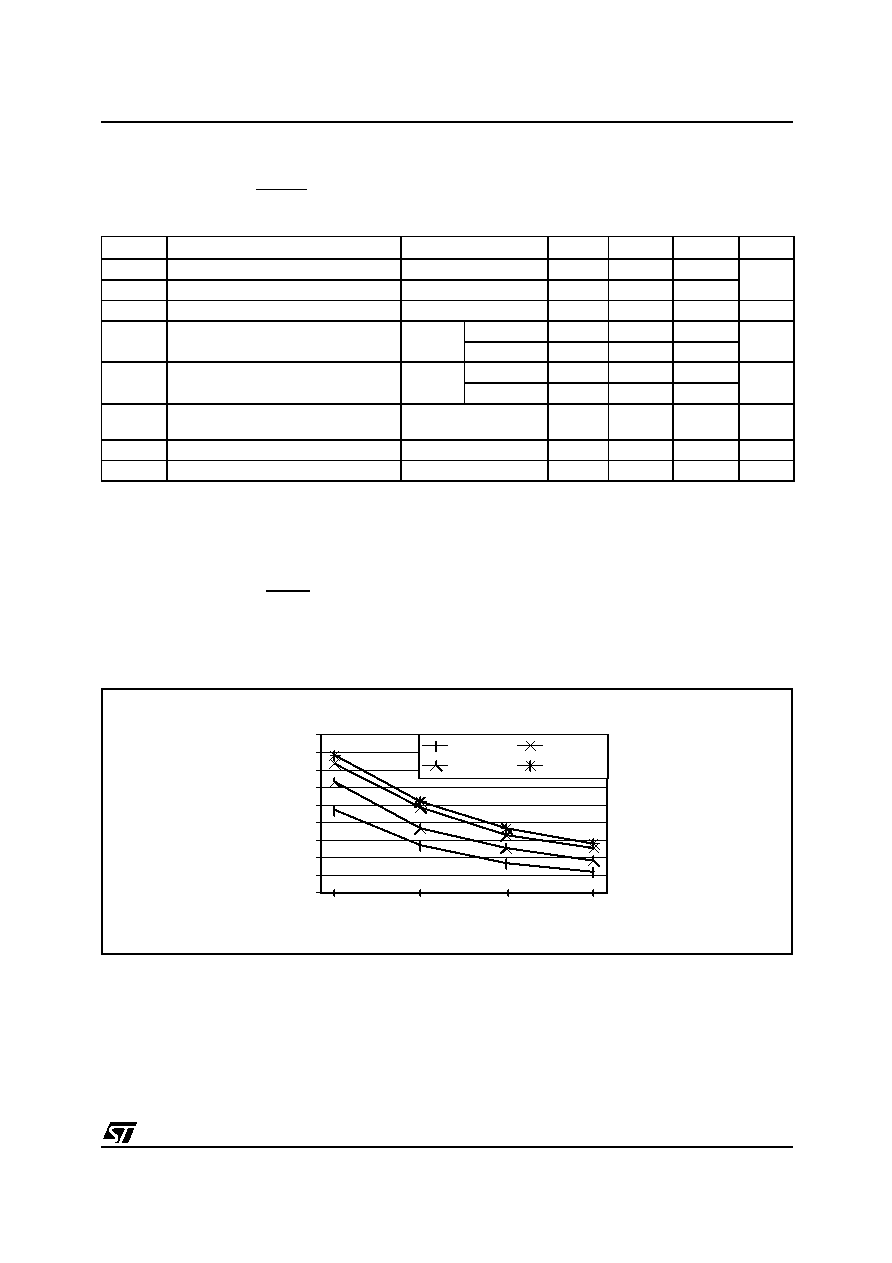
Figure 69. Typical RON vs VDD with VIN=VSS
Symbol
Parameter
Conditions
Min
Typ 1)
Max
Unit
VIL
Input low level voltage 2)
0.3xVDD
V
VIH
Input high level voltage 2)
0.7xVDD
Vhys
Schmitt trigger voltage hysteresis 3)
200
400
mV
RON
Weak pull-up equivalent resistor 4)
VIN=VSS
VDD=5V
150
350
900
k
VDD=3.3V
300
730
1900
RESD
ESD resistor protection
VIN=VSS
VDD=5V
2.8
k
VDD=3.3V
tw(RSTL)out Generated reset pulse duration
External pin or
internal reset sources
tCPU
s
th(RSTL)in External reset pulse hold time
5)
s
tg(RSTL)in Filtered glitch duration
6)
ns
34
56
VDD [V]
100
200
300
400
500
600
700
800
900
1000
Ron [Kohm]
Ta=-40°C
Ta=25°C
Ta=95°C
Ta=125°C
1
相关PDF资料 |
PDF描述 |
|---|---|
| ST62P09CM1/XXX | 8-BIT, MROM, 8 MHz, MICROCONTROLLER, PDSO20 |
| ST62T10CB3 | 8-BIT, OTPROM, 8 MHz, MICROCONTROLLER, PDIP20 |
| ST62T10CM1 | 8-BIT, OTPROM, 8 MHz, MICROCONTROLLER, PDSO20 |
| ST62P20CM1/XXX | 8-BIT, MROM, 8 MHz, MICROCONTROLLER, PDSO20 |
| ST62P20CN1/XXX | 8-BIT, MROM, 8 MHz, MICROCONTROLLER, PDSO20 |
相关代理商/技术参数 |
参数描述 |
|---|---|
| ST62P09CM1/REXTR | 制造商:STMicroelectronics 功能描述: |
| ST62P10CM6/FBS | 制造商:STMicroelectronics 功能描述: |
| ST62P15CM6/AITTR | 制造商:STMicroelectronics 功能描述: |
| ST62P52C | 制造商:STMicroelectronics 功能描述: |
| ST62P62CM6/MOMTR | 制造商:STMicroelectronics 功能描述: |
发布紧急采购,3分钟左右您将得到回复。