- 您现在的位置:买卖IC网 > PDF目录195890 > ST72F324K2 8-BIT MCU WITH NESTED INTERRUPTS. FLASH. 10-BIT ADC. 4 TIMERS. SPI. SCI INTERFACE PDF资料下载
参数资料
| 型号: | ST72F324K2 |
| 英文描述: | 8-BIT MCU WITH NESTED INTERRUPTS. FLASH. 10-BIT ADC. 4 TIMERS. SPI. SCI INTERFACE |
| 中文描述: | 8位微控制器嵌套中断。闪光。 10位ADC。 4定时器。的SPI。 SCI接口 |
| 文件页数: | 41/161页 |
| 文件大小: | 2070K |
| 代理商: | ST72F324K2 |
第1页第2页第3页第4页第5页第6页第7页第8页第9页第10页第11页第12页第13页第14页第15页第16页第17页第18页第19页第20页第21页第22页第23页第24页第25页第26页第27页第28页第29页第30页第31页第32页第33页第34页第35页第36页第37页第38页第39页第40页当前第41页第42页第43页第44页第45页第46页第47页第48页第49页第50页第51页第52页第53页第54页第55页第56页第57页第58页第59页第60页第61页第62页第63页第64页第65页第66页第67页第68页第69页第70页第71页第72页第73页第74页第75页第76页第77页第78页第79页第80页第81页第82页第83页第84页第85页第86页第87页第88页第89页第90页第91页第92页第93页第94页第95页第96页第97页第98页第99页第100页第101页第102页第103页第104页第105页第106页第107页第108页第109页第110页第111页第112页第113页第114页第115页第116页第117页第118页第119页第120页第121页第122页第123页第124页第125页第126页第127页第128页第129页第130页第131页第132页第133页第134页第135页第136页第137页第138页第139页第140页第141页第142页第143页第144页第145页第146页第147页第148页第149页第150页第151页第152页第153页第154页第155页第156页第157页第158页第159页第160页第161页
ST72324
135/161
12.8 I/O PORT PIN CHARACTERISTICS
12.8.1 General Characteristics
Subject to general operating conditions for VDD, fOSC, and TA unless otherwise specified.
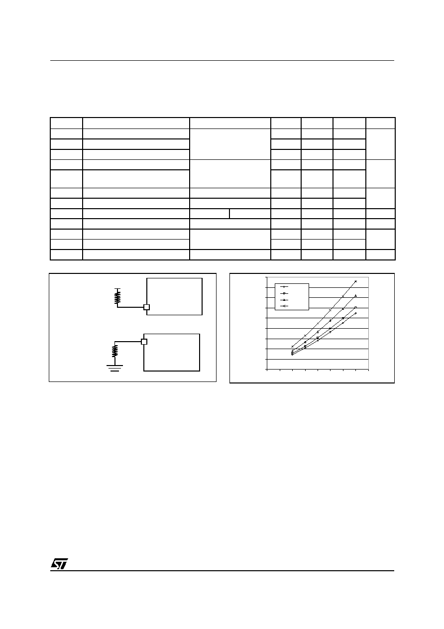
Figure 77. Connecting Unused I/O Pins
Figure 78. Typical IPU vs. VDD with VIN=VSS
Notes:
1. Data based on characterization results, not tested in production.
2. Hysteresis voltage between Schmitt trigger switching levels. Based on characterization results, not tested.
3. When the current limitation is not possible, the VIN maximum must be respected, otherwise refer to IINJ(PIN) specifica-
tion. A positive injection is induced by VIN>VDD while a negative injection is induced by VIN<VSS. Refer to Section 12.2.2
on page 114 for more details.
4. Configuration not recommended, all unused pins must be kept at a fixed voltage: using the output mode of the I/O for
example or an external pull-up or pull-down resistor (see Figure 77). Data based on design simulation and/or technology
characteristics, not tested in production.
5. The RPU pull-up equivalent resistor is based on a resistive transistor (corresponding IPU current characteristics de-
scribed in Figure 78).
6. To generate an external interrupt, a minimum pulse width has to be applied on an I/O port pin configured as an external
interrupt source.
Symbol
Parameter
Conditions
Min
Typ
Max
Unit
VIL
Input low level voltage 1)
CMOS ports
0.3xVDD
V
VIH
Input high level voltage 1)
0.7xVDD
Vhys
Schmitt trigger voltage hysteresis 2)
0.7
IINJ(PIN)
3)
Injected Current on an I/O pin
VDD=5V
± 4
mA
ΣI
INJ(PIN)
3) Total injected current (sum of all I/O
and control pins)
± 25
IL
Input leakage current
VSS≤VIN≤VDD
±1
A
IS
Static current consumption
Floating input mode4)
200
RPU
Weak pull-up equivalent resistor 5)
VIN=VSS
VDD=5V
50
120
250
k
CIO
I/O pin capacitance
5
pF
tf(IO)out
Output high to low level fall time 1)
CL=50pF
Between 10% and 90%
25
ns
tr(IO)out
Output low to high level rise time 1)
25
tw(IT)in
External interrupt pulse time 6)
1tCPU
10k
UNUSED I/O PORT
ST72XXX
10k
UNUSED I/O PORT
ST72XXX
VDD
0
10
20
30
40
50
60
70
80
90
22 .5
33 .5
4
4.5
5
5 .5
6
Vdd(V)
Ip
u(
uA
)
Ta=1 40°C
Ta=9 5°C
Ta=2 5°C
Ta=-45 °C
相关PDF资料 |
PDF描述 |
|---|---|
| ST72F324K4 | 64Mb EDO/FPM - OBSOLETE |
| ST72F324K6 | 64Mb EDO/FPM - OBSOLETE |
| ST72F611F1 | 64Mb EDO/FPM - OBSOLETE |
| ST72F611F1B1 | 64Mb EDO/FPM - OBSOLETE |
| ST72P621L4B1 | LOW SPEED USB 8-BIT MCU WITH 3 ENDPOINTS. FLASH OR ROM MEMORY. LVD. WDG. 10-BIT ADC. 2 TIMERS. SCI. SPI |
相关代理商/技术参数 |
参数描述 |
|---|---|
| ST72F324K2B6 | 功能描述:8位微控制器 -MCU 5V RANGE 8B MCU RoHS:否 制造商:Silicon Labs 核心:8051 处理器系列:C8051F39x 数据总线宽度:8 bit 最大时钟频率:50 MHz 程序存储器大小:16 KB 数据 RAM 大小:1 KB 片上 ADC:Yes 工作电源电压:1.8 V to 3.6 V 工作温度范围:- 40 C to + 105 C 封装 / 箱体:QFN-20 安装风格:SMD/SMT |
| ST72F324K2T3 | 制造商:STMicroelectronics 功能描述: |
| ST72F324K2T3TR | 制造商:STMicroelectronics 功能描述: |
| ST72F324K2T6 | 功能描述:8位微控制器 -MCU Flash 8K SPI/SCI RoHS:否 制造商:Silicon Labs 核心:8051 处理器系列:C8051F39x 数据总线宽度:8 bit 最大时钟频率:50 MHz 程序存储器大小:16 KB 数据 RAM 大小:1 KB 片上 ADC:Yes 工作电源电压:1.8 V to 3.6 V 工作温度范围:- 40 C to + 105 C 封装 / 箱体:QFN-20 安装风格:SMD/SMT |
| ST72F324K2T6TR | 功能描述:8位微控制器 -MCU 8 BITS MICROCONTR RoHS:否 制造商:Silicon Labs 核心:8051 处理器系列:C8051F39x 数据总线宽度:8 bit 最大时钟频率:50 MHz 程序存储器大小:16 KB 数据 RAM 大小:1 KB 片上 ADC:Yes 工作电源电压:1.8 V to 3.6 V 工作温度范围:- 40 C to + 105 C 封装 / 箱体:QFN-20 安装风格:SMD/SMT |
发布紧急采购,3分钟左右您将得到回复。