- 您现在的位置:买卖IC网 > PDF目录195890 > ST72F324K2 8-BIT MCU WITH NESTED INTERRUPTS. FLASH. 10-BIT ADC. 4 TIMERS. SPI. SCI INTERFACE PDF资料下载
参数资料
| 型号: | ST72F324K2 |
| 英文描述: | 8-BIT MCU WITH NESTED INTERRUPTS. FLASH. 10-BIT ADC. 4 TIMERS. SPI. SCI INTERFACE |
| 中文描述: | 8位微控制器嵌套中断。闪光。 10位ADC。 4定时器。的SPI。 SCI接口 |
| 文件页数: | 50/161页 |
| 文件大小: | 2070K |
| 代理商: | ST72F324K2 |
第1页第2页第3页第4页第5页第6页第7页第8页第9页第10页第11页第12页第13页第14页第15页第16页第17页第18页第19页第20页第21页第22页第23页第24页第25页第26页第27页第28页第29页第30页第31页第32页第33页第34页第35页第36页第37页第38页第39页第40页第41页第42页第43页第44页第45页第46页第47页第48页第49页当前第50页第51页第52页第53页第54页第55页第56页第57页第58页第59页第60页第61页第62页第63页第64页第65页第66页第67页第68页第69页第70页第71页第72页第73页第74页第75页第76页第77页第78页第79页第80页第81页第82页第83页第84页第85页第86页第87页第88页第89页第90页第91页第92页第93页第94页第95页第96页第97页第98页第99页第100页第101页第102页第103页第104页第105页第106页第107页第108页第109页第110页第111页第112页第113页第114页第115页第116页第117页第118页第119页第120页第121页第122页第123页第124页第125页第126页第127页第128页第129页第130页第131页第132页第133页第134页第135页第136页第137页第138页第139页第140页第141页第142页第143页第144页第145页第146页第147页第148页第149页第150页第151页第152页第153页第154页第155页第156页第157页第158页第159页第160页第161页
ST72324
143/161
ADC CHARACTERISTICS (Cont’d)
12.12.1 Analog Power Supply and Reference
Pins
Depending on the MCU pin count, the package
may feature separate VAREF and VSSA analog
power supply pins. These pins supply power to the
A/D converter cell and function as the high and low
reference voltages for the conversion. In some
packages, VAREF and VSSA pins are not available
(refer to Table 1). In this case the analog supply
and reference pads are internally bonded to the
VDD and VSS pins.
Separation of the digital and analog power pins al-
low board designers to improve A/D performance.
Conversion accuracy can be impacted by voltage
drops and noise in the event of heavily loaded or
badly decoupled power supply lines (see Section
12.12.2 General PCB Design Guidelines
To obtain best results, some general design and
layout rules should be followed when designing
the application PCB to shield the noise-sensitive,
analog physical interface from noise-generating
CMOS logic signals.
– Use separate digital and analog planes. The an-
alog ground plane should be connected to the
digital ground plane via a single point on the
PCB.
– Filter power to the analog power planes. It is rec-
ommended to connect capacitors, with good high
frequency characteristics, between the power
and ground lines, placing 0.1F and optionally, if
needed 10pF capacitors as close as possible to
the ST7 power supply pins and a 1 to 10F ca-
pacitor close to the power source (see Figure
– The analog and digital power supplies should be
connected in a star nework. Do not use a resis-
tor, as VAREF is used as a reference voltage by
the A/D converter and any resistance would
cause a voltage drop and a loss of accuracy.
– Properly place components and route the signal
traces on the PCB to shield the analog inputs.
Analog signals paths should run over the analog
ground plane and be as short as possible. Isolate
analog signals from digital signals that may
switch while the analog inputs are being sampled
by the A/D converter. Do not toggle digital out-
puts on the same I/O port as the A/D input being
converted.
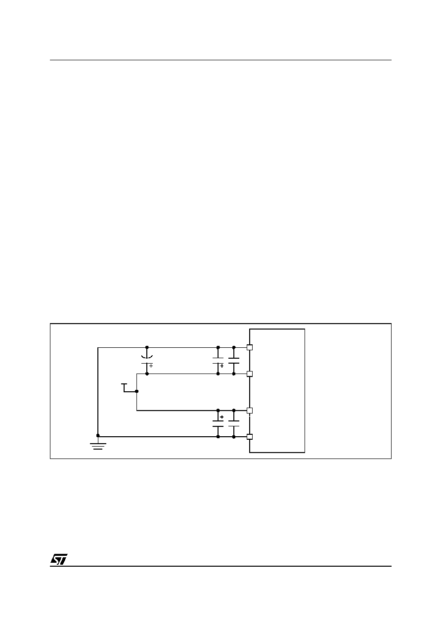
Figure 93. Power Supply Filtering
VSS
VDD
0.1
F
10pF
VDD
ST72XXX
VAREF
VSSA
POWER
SUPPLY
SOURCE
ST7
DIGITAL NOISE
FILTERING
EXTERNAL
NOISE
FILTERING
1 to 10
F
0.1
F
10pF
(if needed)
相关PDF资料 |
PDF描述 |
|---|---|
| ST72F324K4 | 64Mb EDO/FPM - OBSOLETE |
| ST72F324K6 | 64Mb EDO/FPM - OBSOLETE |
| ST72F611F1 | 64Mb EDO/FPM - OBSOLETE |
| ST72F611F1B1 | 64Mb EDO/FPM - OBSOLETE |
| ST72P621L4B1 | LOW SPEED USB 8-BIT MCU WITH 3 ENDPOINTS. FLASH OR ROM MEMORY. LVD. WDG. 10-BIT ADC. 2 TIMERS. SCI. SPI |
相关代理商/技术参数 |
参数描述 |
|---|---|
| ST72F324K2B6 | 功能描述:8位微控制器 -MCU 5V RANGE 8B MCU RoHS:否 制造商:Silicon Labs 核心:8051 处理器系列:C8051F39x 数据总线宽度:8 bit 最大时钟频率:50 MHz 程序存储器大小:16 KB 数据 RAM 大小:1 KB 片上 ADC:Yes 工作电源电压:1.8 V to 3.6 V 工作温度范围:- 40 C to + 105 C 封装 / 箱体:QFN-20 安装风格:SMD/SMT |
| ST72F324K2T3 | 制造商:STMicroelectronics 功能描述: |
| ST72F324K2T3TR | 制造商:STMicroelectronics 功能描述: |
| ST72F324K2T6 | 功能描述:8位微控制器 -MCU Flash 8K SPI/SCI RoHS:否 制造商:Silicon Labs 核心:8051 处理器系列:C8051F39x 数据总线宽度:8 bit 最大时钟频率:50 MHz 程序存储器大小:16 KB 数据 RAM 大小:1 KB 片上 ADC:Yes 工作电源电压:1.8 V to 3.6 V 工作温度范围:- 40 C to + 105 C 封装 / 箱体:QFN-20 安装风格:SMD/SMT |
| ST72F324K2T6TR | 功能描述:8位微控制器 -MCU 8 BITS MICROCONTR RoHS:否 制造商:Silicon Labs 核心:8051 处理器系列:C8051F39x 数据总线宽度:8 bit 最大时钟频率:50 MHz 程序存储器大小:16 KB 数据 RAM 大小:1 KB 片上 ADC:Yes 工作电源电压:1.8 V to 3.6 V 工作温度范围:- 40 C to + 105 C 封装 / 箱体:QFN-20 安装风格:SMD/SMT |
发布紧急采购,3分钟左右您将得到回复。