- 您现在的位置:买卖IC网 > PDF目录98145 > ST72F345N4H6 (STMICROELECTRONICS) 8-BIT, FLASH, 8 MHz, MICROCONTROLLER, PBGA56 PDF资料下载
参数资料
| 型号: | ST72F345N4H6 |
| 厂商: | STMICROELECTRONICS |
| 元件分类: | 微控制器/微处理器 |
| 英文描述: | 8-BIT, FLASH, 8 MHz, MICROCONTROLLER, PBGA56 |
| 封装: | 6 X 6 MM, LEAD FREE, TFBGA-56 |
| 文件页数: | 10/190页 |
| 文件大小: | 3666K |
| 代理商: | ST72F345N4H6 |
第1页第2页第3页第4页第5页第6页第7页第8页第9页当前第10页第11页第12页第13页第14页第15页第16页第17页第18页第19页第20页第21页第22页第23页第24页第25页第26页第27页第28页第29页第30页第31页第32页第33页第34页第35页第36页第37页第38页第39页第40页第41页第42页第43页第44页第45页第46页第47页第48页第49页第50页第51页第52页第53页第54页第55页第56页第57页第58页第59页第60页第61页第62页第63页第64页第65页第66页第67页第68页第69页第70页第71页第72页第73页第74页第75页第76页第77页第78页第79页第80页第81页第82页第83页第84页第85页第86页第87页第88页第89页第90页第91页第92页第93页第94页第95页第96页第97页第98页第99页第100页第101页第102页第103页第104页第105页第106页第107页第108页第109页第110页第111页第112页第113页第114页第115页第116页第117页第118页第119页第120页第121页第122页第123页第124页第125页第126页第127页第128页第129页第130页第131页第132页第133页第134页第135页第136页第137页第138页第139页第140页第141页第142页第143页第144页第145页第146页第147页第148页第149页第150页第151页第152页第153页第154页第155页第156页第157页第158页第159页第160页第161页第162页第163页第164页第165页第166页第167页第168页第169页第170页第171页第172页第173页第174页第175页第176页第177页第178页第179页第180页第181页第182页第183页第184页第185页第186页第187页第188页第189页第190页
ST72340, ST72344, ST72345
107/190
SCI SERIAL COMMUNICATION INTERFACE (Cont’d)
11.5.4.7 Parity control
Parity control (generation of parity bit in trasmis-
sion and and parity checking in reception) can be
enabled by setting the PCE bit in the SCICR1 reg-
ister. Depending on the frame length defined by
the M bit, the possible SCI frame formats are as
listed in Table 21.
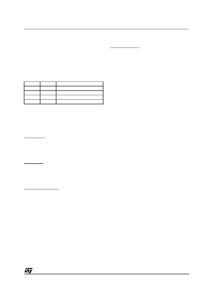
Table 21. Frame Formats
Legend:
SB : Start Bit
STB : Stop Bit
PB : Parity Bit
Note: In case of wake up by an address mark, the
MSB bit of the data is taken into account and not
the parity bit
Even parity: the parity bit is calculated to obtain
an even number of “1s” inside the frame made of
the 7 or 8 LSB bits (depending on whether M is
equal to 0 or 1) and the parity bit.
Ex: data=00110101; 4 bits set => parity bit will be
0 if even parity is selected (PS bit = 0).
Odd parity: the parity bit is calculated to obtain an
odd number of “1s” inside the frame made of the 7
or 8 LSB bits (depending on whether M is equal to
0 or 1) and the parity bit.
Ex: data=00110101; 4 bits set => parity bit will be
1 if odd parity is selected (PS bit = 1).
Transmission mode: If the PCE bit is set then the
MSB bit of the data written in the data register is
not transmitted but is changed by the parity bit.
Reception mode: If the PCE bit is set then the in-
terface checks if the received data byte has an
even number of “1s” if even parity is selected
(PS=0) or an odd number of “1s” if odd parity is se-
lected (PS=1). If the parity check fails, the PE flag
is set in the SCISR register and an interrupt is gen-
erated if PIE is set in the SCICR1 register.
11.5.4.8 SCI Clock Tolerance
During reception, each bit is sampled 16 times.
The majority of the 8th, 9th and 10th samples is
considered as the bit value. For a valid bit detec-
tion, all the three samples should have the same
value otherwise the noise flag (NF) is set. For ex-
ample: if the 8th, 9th and 10th samples are 0, 1
and 1 respectively, then the bit value will be “1”,
but the Noise Flag bit is be set because the three
samples values are not the same.
Consequently, the bit length must be long enough
so that the 8th, 9th and 10th samples have the de-
sired bit value. This means the clock frequency
should not vary more than 6/16 (37.5%) within one
bit. The sampling clock is resynchronized at each
start bit, so that when receiving 10 bits (one start
bit, 1 data byte, 1 stop bit), the clock deviation
must not exceed 3.75%.
Note: The internal sampling clock of the microcon-
troller samples the pin value on every falling edge.
Therefore, the internal sampling clock and the time
the application expects the sampling to take place
may be out of sync. For example: If the baud rate
is 15.625 kbaud (bit length is 64s), then the 8th,
9th and 10th samples will be at 28s, 32s & 36s
respectively (the first sample starting ideally at
0s). But if the falling edge of the internal clock oc-
curs just before the pin value changes, the sam-
ples would then be out of sync by ~4us. This
means the entire bit length must be at least 40s
(36s for the 10th sample + 4s for synchroniza-
tion with the internal sampling clock).
M bit
PCE bit
SCI frame
0
| SB | 8 bit data | STB |
0
1
| SB | 7-bit data | PB | STB |
1
0
| SB | 9-bit data | STB |
1
| SB | 8-bit data PB | STB |
相关PDF资料 |
PDF描述 |
|---|---|
| ST72F60E1M1 | 8-BIT, FLASH, 8 MHz, MICROCONTROLLER, PDSO24 |
| ST72F60K2DIE1 | 8-BIT, MROM, 8 MHz, MICROCONTROLLER, UUC |
| ST72F60K2DIE6 | 8-BIT, MROM, 8 MHz, MICROCONTROLLER, UUC |
| ST72F651AR6T1 | 8-BIT, FLASH, MICROCONTROLLER, PQFP64 |
| ST72P60E2M1 | 8-BIT, MROM, 8 MHz, MICROCONTROLLER, PDSO24 |
相关代理商/技术参数 |
参数描述 |
|---|---|
| ST72F34X-SK/RAIS | 功能描述:开发板和工具包 - 其他处理器 DEV. KIT RoHS:否 制造商:Freescale Semiconductor 产品:Development Systems 工具用于评估:P3041 核心:e500mc 接口类型:I2C, SPI, USB 工作电源电压: |
| ST72F361AR6T3 | 功能描述:8位微控制器 -MCU 8B MCU with Flash RoHS:否 制造商:Silicon Labs 核心:8051 处理器系列:C8051F39x 数据总线宽度:8 bit 最大时钟频率:50 MHz 程序存储器大小:16 KB 数据 RAM 大小:1 KB 片上 ADC:Yes 工作电源电压:1.8 V to 3.6 V 工作温度范围:- 40 C to + 105 C 封装 / 箱体:QFN-20 安装风格:SMD/SMT |
| ST72F361AR6T6 | 功能描述:8位微控制器 -MCU 8-bit MCU with Flash or ROM 10-bit ADC RoHS:否 制造商:Silicon Labs 核心:8051 处理器系列:C8051F39x 数据总线宽度:8 bit 最大时钟频率:50 MHz 程序存储器大小:16 KB 数据 RAM 大小:1 KB 片上 ADC:Yes 工作电源电压:1.8 V to 3.6 V 工作温度范围:- 40 C to + 105 C 封装 / 箱体:QFN-20 安装风格:SMD/SMT |
| ST72F361AR6TA | 功能描述:8位微控制器 -MCU 8-bit MCU Flash RoHS:否 制造商:Silicon Labs 核心:8051 处理器系列:C8051F39x 数据总线宽度:8 bit 最大时钟频率:50 MHz 程序存储器大小:16 KB 数据 RAM 大小:1 KB 片上 ADC:Yes 工作电源电压:1.8 V to 3.6 V 工作温度范围:- 40 C to + 105 C 封装 / 箱体:QFN-20 安装风格:SMD/SMT |
| ST72F361AR6TAE | 功能描述:8位微控制器 -MCU 8B MCU with Flash RoHS:否 制造商:Silicon Labs 核心:8051 处理器系列:C8051F39x 数据总线宽度:8 bit 最大时钟频率:50 MHz 程序存储器大小:16 KB 数据 RAM 大小:1 KB 片上 ADC:Yes 工作电源电压:1.8 V to 3.6 V 工作温度范围:- 40 C to + 105 C 封装 / 箱体:QFN-20 安装风格:SMD/SMT |
发布紧急采购,3分钟左右您将得到回复。