- 您现在的位置:买卖IC网 > PDF目录195890 > ST72F611F1B1 64Mb EDO/FPM - OBSOLETE PDF资料下载
参数资料
| 型号: | ST72F611F1B1 |
| 英文描述: | 64Mb EDO/FPM - OBSOLETE |
| 中文描述: | ST7的-低速USB 8 - 3端点位MCU。闪存。内径。水分散粒剂。定时器 |
| 文件页数: | 160/161页 |
| 文件大小: | 2070K |
| 代理商: | ST72F611F1B1 |
第1页第2页第3页第4页第5页第6页第7页第8页第9页第10页第11页第12页第13页第14页第15页第16页第17页第18页第19页第20页第21页第22页第23页第24页第25页第26页第27页第28页第29页第30页第31页第32页第33页第34页第35页第36页第37页第38页第39页第40页第41页第42页第43页第44页第45页第46页第47页第48页第49页第50页第51页第52页第53页第54页第55页第56页第57页第58页第59页第60页第61页第62页第63页第64页第65页第66页第67页第68页第69页第70页第71页第72页第73页第74页第75页第76页第77页第78页第79页第80页第81页第82页第83页第84页第85页第86页第87页第88页第89页第90页第91页第92页第93页第94页第95页第96页第97页第98页第99页第100页第101页第102页第103页第104页第105页第106页第107页第108页第109页第110页第111页第112页第113页第114页第115页第116页第117页第118页第119页第120页第121页第122页第123页第124页第125页第126页第127页第128页第129页第130页第131页第132页第133页第134页第135页第136页第137页第138页第139页第140页第141页第142页第143页第144页第145页第146页第147页第148页第149页第150页第151页第152页第153页第154页第155页第156页第157页第158页第159页当前第160页第161页
ST72324
98/161
SERIAL COMMUNICATIONS INTERFACE (Cont’d)
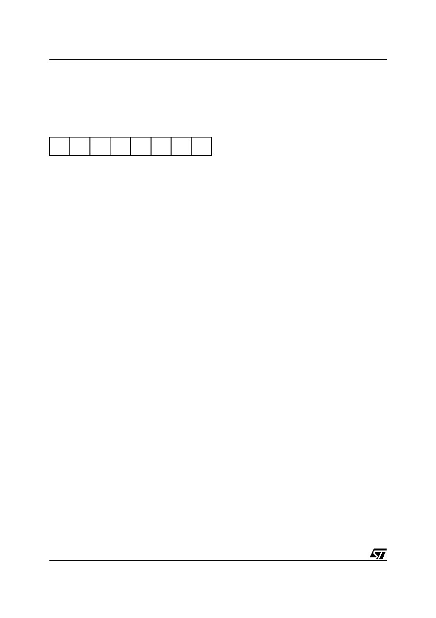
CONTROL REGISTER 1 (SCICR1)
Read/Write
Reset Value: x000 0000 (x0h)
Bit 7 = R8
Receive data bit 8.
This bit is used to store the 9th bit of the received
word when M=1.
Bit 6 = T8
Transmit data bit 8.
This bit is used to store the 9th bit of the transmit-
ted word when M=1.
Bit 5 = SCID
Disabled for low power consumption
When this bit is set the SCI prescalers and outputs
are stopped and the end of the current byte trans-
fer in order to reduce power consumption.This bit
is set and cleared by software.
0: SCI enabled
1: SCI prescaler and outputs disabled
Bit 4 = M
Word length.
This bit determines the word length. It is set or
cleared by software.
0: 1 Start bit, 8 Data bits, 1 Stop bit
1: 1 Start bit, 9 Data bits, 1 Stop bit
Note: The M bit must not be modified during a data
transfer (both transmission and reception).
Bit 3 = WAKE
Wake-Up method.
This bit determines the SCI Wake-Up method, it is
set or cleared by software.
0: Idle Line
1: Address Mark
Bit 2 = PCE
Parity control enable.
This bit selects the hardware parity control (gener-
ation and detection). When the parity control is en-
abled, the computed parity is inserted at the MSB
position (9th bit if M=1; 8th bit if M=0) and parity is
checked on the received data. This bit is set and
cleared by software. Once it is set, PCE is active
after the current byte (in reception and in transmis-
sion).
0: Parity control disabled
1: Parity control enabled
Bit 1 = PS
Parity selection.
This bit selects the odd or even parity when the
parity generation/detection is enabled (PCE bit
set). It is set and cleared by software. The parity
will be selected after the current byte.
0: Even parity
1: Odd parity
Bit 0 = PIE
Parity interrupt enable.
This bit enables the interrupt capability of the hard-
ware parity control when a parity error is detected
(PE bit set). It is set and cleared by software.
0: Parity error interrupt disabled
1: Parity error interrupt enabled.
70
R8
T8
SCID
M
WAKE
PCE
PS
PIE
相关PDF资料 |
PDF描述 |
|---|---|
| ST72P621L4B1 | LOW SPEED USB 8-BIT MCU WITH 3 ENDPOINTS. FLASH OR ROM MEMORY. LVD. WDG. 10-BIT ADC. 2 TIMERS. SCI. SPI |
| ST72T213G1B3 | 8-BIT MCU WITH 4 TO 8K ROM/OTP/EPROM, 256 BYTES RAM, ADC, WDG, SPI AND 1 OR 2 TIMERS |
| ST72T213G1B6 | 8-BIT MCU WITH 4 TO 8K ROM/OTP/EPROM, 256 BYTES RAM, ADC, WDG, SPI AND 1 OR 2 TIMERS |
| ST72T213G1M3 | 8-BIT MCU WITH 4 TO 8K ROM/OTP/EPROM, 256 BYTES RAM, ADC, WDG, SPI AND 1 OR 2 TIMERS |
| ST72T213G1M6 | 8-BIT MCU WITH 4 TO 8K ROM/OTP/EPROM, 256 BYTES RAM, ADC, WDG, SPI AND 1 OR 2 TIMERS |
相关代理商/技术参数 |
参数描述 |
|---|---|
| ST72F621J4B1 | 功能描述:8位微控制器 -MCU Flash 16K USB/SPI/SC RoHS:否 制造商:Silicon Labs 核心:8051 处理器系列:C8051F39x 数据总线宽度:8 bit 最大时钟频率:50 MHz 程序存储器大小:16 KB 数据 RAM 大小:1 KB 片上 ADC:Yes 工作电源电压:1.8 V to 3.6 V 工作温度范围:- 40 C to + 105 C 封装 / 箱体:QFN-20 安装风格:SMD/SMT |
| ST72F621J4D0 | 功能描述:8位微控制器 -MCU Flash 16K USB/SPI/SC RoHS:否 制造商:Silicon Labs 核心:8051 处理器系列:C8051F39x 数据总线宽度:8 bit 最大时钟频率:50 MHz 程序存储器大小:16 KB 数据 RAM 大小:1 KB 片上 ADC:Yes 工作电源电压:1.8 V to 3.6 V 工作温度范围:- 40 C to + 105 C 封装 / 箱体:QFN-20 安装风格:SMD/SMT |
| ST72F621J4T1 | 功能描述:8位微控制器 -MCU ST7262 Lo Spd USB 8B MCU RoHS:否 制造商:Silicon Labs 核心:8051 处理器系列:C8051F39x 数据总线宽度:8 bit 最大时钟频率:50 MHz 程序存储器大小:16 KB 数据 RAM 大小:1 KB 片上 ADC:Yes 工作电源电压:1.8 V to 3.6 V 工作温度范围:- 40 C to + 105 C 封装 / 箱体:QFN-20 安装风格:SMD/SMT |
| ST72F621K4B1 | 功能描述:8位微控制器 -MCU Flash 16K USB/SPI/SC RoHS:否 制造商:Silicon Labs 核心:8051 处理器系列:C8051F39x 数据总线宽度:8 bit 最大时钟频率:50 MHz 程序存储器大小:16 KB 数据 RAM 大小:1 KB 片上 ADC:Yes 工作电源电压:1.8 V to 3.6 V 工作温度范围:- 40 C to + 105 C 封装 / 箱体:QFN-20 安装风格:SMD/SMT |
| ST72F621L4M1 | 功能描述:8位微控制器 -MCU Flash 16K USB/SPI/SC RoHS:否 制造商:Silicon Labs 核心:8051 处理器系列:C8051F39x 数据总线宽度:8 bit 最大时钟频率:50 MHz 程序存储器大小:16 KB 数据 RAM 大小:1 KB 片上 ADC:Yes 工作电源电压:1.8 V to 3.6 V 工作温度范围:- 40 C to + 105 C 封装 / 箱体:QFN-20 安装风格:SMD/SMT |
发布紧急采购,3分钟左右您将得到回复。