- 您现在的位置:买卖IC网 > PDF目录69373 > ST7FL38F2MAE (STMICROELECTRONICS) 8-BIT, FLASH, 8 MHz, MICROCONTROLLER, PDSO20 PDF资料下载
参数资料
| 型号: | ST7FL38F2MAE |
| 厂商: | STMICROELECTRONICS |
| 元件分类: | 微控制器/微处理器 |
| 英文描述: | 8-BIT, FLASH, 8 MHz, MICROCONTROLLER, PDSO20 |
| 封装: | 0.300 INCH, ROHS COMPLIANT, PLASTIC, SOP-20 |
| 文件页数: | 111/236页 |
| 文件大小: | 2064K |
| 代理商: | ST7FL38F2MAE |
第1页第2页第3页第4页第5页第6页第7页第8页第9页第10页第11页第12页第13页第14页第15页第16页第17页第18页第19页第20页第21页第22页第23页第24页第25页第26页第27页第28页第29页第30页第31页第32页第33页第34页第35页第36页第37页第38页第39页第40页第41页第42页第43页第44页第45页第46页第47页第48页第49页第50页第51页第52页第53页第54页第55页第56页第57页第58页第59页第60页第61页第62页第63页第64页第65页第66页第67页第68页第69页第70页第71页第72页第73页第74页第75页第76页第77页第78页第79页第80页第81页第82页第83页第84页第85页第86页第87页第88页第89页第90页第91页第92页第93页第94页第95页第96页第97页第98页第99页第100页第101页第102页第103页第104页第105页第106页第107页第108页第109页第110页当前第111页第112页第113页第114页第115页第116页第117页第118页第119页第120页第121页第122页第123页第124页第125页第126页第127页第128页第129页第130页第131页第132页第133页第134页第135页第136页第137页第138页第139页第140页第141页第142页第143页第144页第145页第146页第147页第148页第149页第150页第151页第152页第153页第154页第155页第156页第157页第158页第159页第160页第161页第162页第163页第164页第165页第166页第167页第168页第169页第170页第171页第172页第173页第174页第175页第176页第177页第178页第179页第180页第181页第182页第183页第184页第185页第186页第187页第188页第189页第190页第191页第192页第193页第194页第195页第196页第197页第198页第199页第200页第201页第202页第203页第204页第205页第206页第207页第208页第209页第210页第211页第212页第213页第214页第215页第216页第217页第218页第219页第220页第221页第222页第223页第224页第225页第226页第227页第228页第229页第230页第231页第232页第233页第234页第235页第236页
ST7L34, ST7L35, ST7L38, ST7L39
Electrical characteristics
Doc ID 11928 Rev 7
199/236
Designing hardened software to avoid noise problems
EMC characterization and optimization are performed at component level with a typical
application environment and simplified MCU software. It should be noted that good EMC
performance is highly dependent on the user application and the software in particular.
Therefore it is recommended that the user applies EMC software optimization and
prequalification tests in relation with the EMC level requested for his application.
Software recommendations
The software flowchart must include the management of runaway conditions such as:
●
Corrupted program counter
●
Unexpected reset
●
Critical data corruption (control registers...)
Prequalification trials
Most of the common failures (unexpected reset and program counter corruption) can be
reproduced by manually forcing a low state on the reset pin or the oscillator pins for 1
second.
To complete these trials, ESD stress can be applied directly on the device, over the range of
specification values. When unexpectedbehavior is detected, the software can be hardened
to prevent unrecoverable errors occurring (see application note AN1015).
13.7.2
Electromagnetic interference (EMI)
Based on a simple application running on the product (toggling 2 LEDs through the I/O
ports), the product is monitored in terms of emission. This emission test is in line with the
norm SAE J 1752/3 which specifies the board and the loading of each pin. See Table 117:
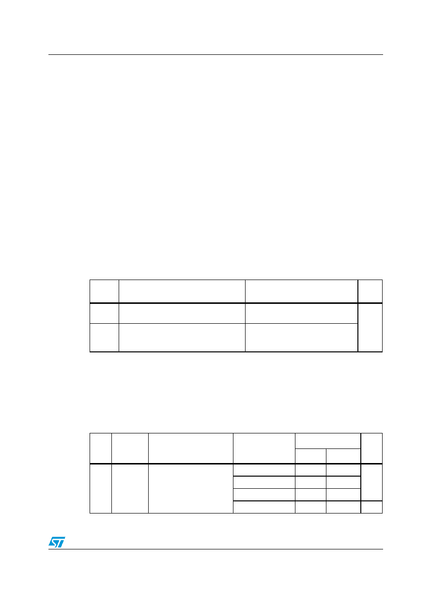
Table 116.
Electromagnetic test results
Symbol
Parameter
Conditions
Level/
class
VFESD
Voltage limits to be applied on any I/O pin
to induce a functional disturbance
VDD = 5 V, TA = 25 °C, fOSC = 8MHz,
conforms to IEC 1000-4-2
3B
VFFTB
Fast transient voltage burst limits to be
applied through 100 pF on VDD and VDD
pins to induce a functional disturbance
VDD = 5 V, TA = 25 °C, fOSC = 8MHz,
conforms to IEC 1000-4-4
Table 117.
EMI emissions
Sym. Parameter
Conditions
Monitored
frequency band
Max vs. [fOSC/fCPU]
Unit
8/4 MHz
16/8 MHz
SEMI
Peak
level(1)
1.
Data based on characterization results, not tested in production.
VDD = 5 V, TA = 25 °C,
SO20 package,
conforming to SAE J 1752/3
0.1MHz to 30 MHz
15
dBV
30 MHz to 130 MHz
13
19
130 MHz to 1 GHz
9
13
SAE EMI level
2.5
3
-
相关PDF资料 |
PDF描述 |
|---|---|
| ST7FL35F2UCRE | 8-BIT, FLASH, 8 MHz, MICROCONTROLLER, QCC20 |
| ST7FL38F2MAXE | 8-BIT, FLASH, 8 MHz, MICROCONTROLLER, PDSO20 |
| ST7FL38F2UAE | 8-BIT, FLASH, 8 MHz, MICROCONTROLLER, QCC20 |
| ST7L35MA/XXXR | 8-BIT, MROM, 8 MHz, MICROCONTROLLER, PDSO20 |
| ST7L35UA/XXXRS | 8-BIT, MROM, 8 MHz, MICROCONTROLLER, QCC20 |
相关代理商/技术参数 |
参数描述 |
|---|---|
| ST7FL38F2MCE | 制造商:STMicroelectronics 功能描述: |
| ST7FL39F2MAE | 功能描述:8位微控制器 -MCU 8-bit MCU Automotive RoHS:否 制造商:Silicon Labs 核心:8051 处理器系列:C8051F39x 数据总线宽度:8 bit 最大时钟频率:50 MHz 程序存储器大小:16 KB 数据 RAM 大小:1 KB 片上 ADC:Yes 工作电源电压:1.8 V to 3.6 V 工作温度范围:- 40 C to + 105 C 封装 / 箱体:QFN-20 安装风格:SMD/SMT |
| ST7FL39F2MC | 制造商:STMicroelectronics 功能描述: |
| ST7FL39F2MCE | 制造商:STMicroelectronics 功能描述: |
| ST7FL39F2MCTR | 制造商:STMicroelectronics 功能描述: |
发布紧急采购,3分钟左右您将得到回复。