- 您现在的位置:买卖IC网 > PDF目录98146 > ST90158M9T1 (STMICROELECTRONICS) 16-BIT, MROM, 14 MHz, MICROCONTROLLER, PQFP80 PDF资料下载
参数资料
| 型号: | ST90158M9T1 |
| 厂商: | STMICROELECTRONICS |
| 元件分类: | 微控制器/微处理器 |
| 英文描述: | 16-BIT, MROM, 14 MHz, MICROCONTROLLER, PQFP80 |
| 封装: | PLASTIC, TQFP-80 |
| 文件页数: | 170/190页 |
| 文件大小: | 1152K |
| 代理商: | ST90158M9T1 |
第1页第2页第3页第4页第5页第6页第7页第8页第9页第10页第11页第12页第13页第14页第15页第16页第17页第18页第19页第20页第21页第22页第23页第24页第25页第26页第27页第28页第29页第30页第31页第32页第33页第34页第35页第36页第37页第38页第39页第40页第41页第42页第43页第44页第45页第46页第47页第48页第49页第50页第51页第52页第53页第54页第55页第56页第57页第58页第59页第60页第61页第62页第63页第64页第65页第66页第67页第68页第69页第70页第71页第72页第73页第74页第75页第76页第77页第78页第79页第80页第81页第82页第83页第84页第85页第86页第87页第88页第89页第90页第91页第92页第93页第94页第95页第96页第97页第98页第99页第100页第101页第102页第103页第104页第105页第106页第107页第108页第109页第110页第111页第112页第113页第114页第115页第116页第117页第118页第119页第120页第121页第122页第123页第124页第125页第126页第127页第128页第129页第130页第131页第132页第133页第134页第135页第136页第137页第138页第139页第140页第141页第142页第143页第144页第145页第146页第147页第148页第149页第150页第151页第152页第153页第154页第155页第156页第157页第158页第159页第160页第161页第162页第163页第164页第165页第166页第167页第168页第169页当前第170页第171页第172页第173页第174页第175页第176页第177页第178页第179页第180页第181页第182页第183页第184页第185页第186页第187页第188页第189页第190页
80/190
ST90158 - RESET AND CLOCK CONTROL UNIT (RCCU)
RESET/STOP MANAGER (Cont’d)
The on-chip Timer/Watchdog generates a reset
condition if the Watchdog mode is enabled
(WCR.WDEN cleared, R252 page 0), and if the
programmed period elapses without the specific
code (AAh, 55h) written to the appropriate register.
The input pin RESET is not driven low by the on-
chip reset generated by the Timer/Watchdog.
When the RESET pin goes high again, 510 oscilla-
tor clock cycles (CLOCK1) are counted before ex-
iting the Reset state (+-1 CLOCK1 period, depend-
ing on the delay between the rising edge of the RE-
SET pin and the first rising edge of CLOCK1). Sub-
sequently a short Boot routine is executed from the
device internal Boot ROM, and control then passes
to the user program.
The Boot routine sets the device characteristics
and loads the correct values in the Memory Man-
agement Unit’s pointer registers, so that these
point to the physical memory areas as mapped in
the specific device. The precise duration of this
short Boot routine varies from device to device,
depending on the Boot ROM contents.
At the end of the Boot routine the Program Coun-
ter will be set to the location specified in the Reset
Vector located in the lowest two bytes of memory.
6.6.1 RESET Pin Timing
To improve the noise immunity of the device, the
RESET pin has a Schmitt trigger input circuit with
hysteresis. In addition, a filter will prevent an un-
wanted reset in case of a single glitch of less than
50 ns on the RESET pin. The device is certain to
reset if a negative pulse of more than 20
s is ap-
plied. When the RESET pin goes high again, a de-
lay of up to 4
s will elapse before the RCCU de-
tects this rising front. From this event on, 510 os-
cillator clock cycles (CLOCK1) are counted before
exiting the Reset state (+-1CLOCK1 period de-
pending on the delay between the positive edge
the RCCU detects and the first rising edge of
CLOCK1)
If the ST9 is a ROMLESS version, without on-chip
program memory, the mermory interface ports are
set to external memory mode (i.e Alternate Func-
tion) and the memory accesses are made to exter-
nal Program memory with wait cycles insertion.
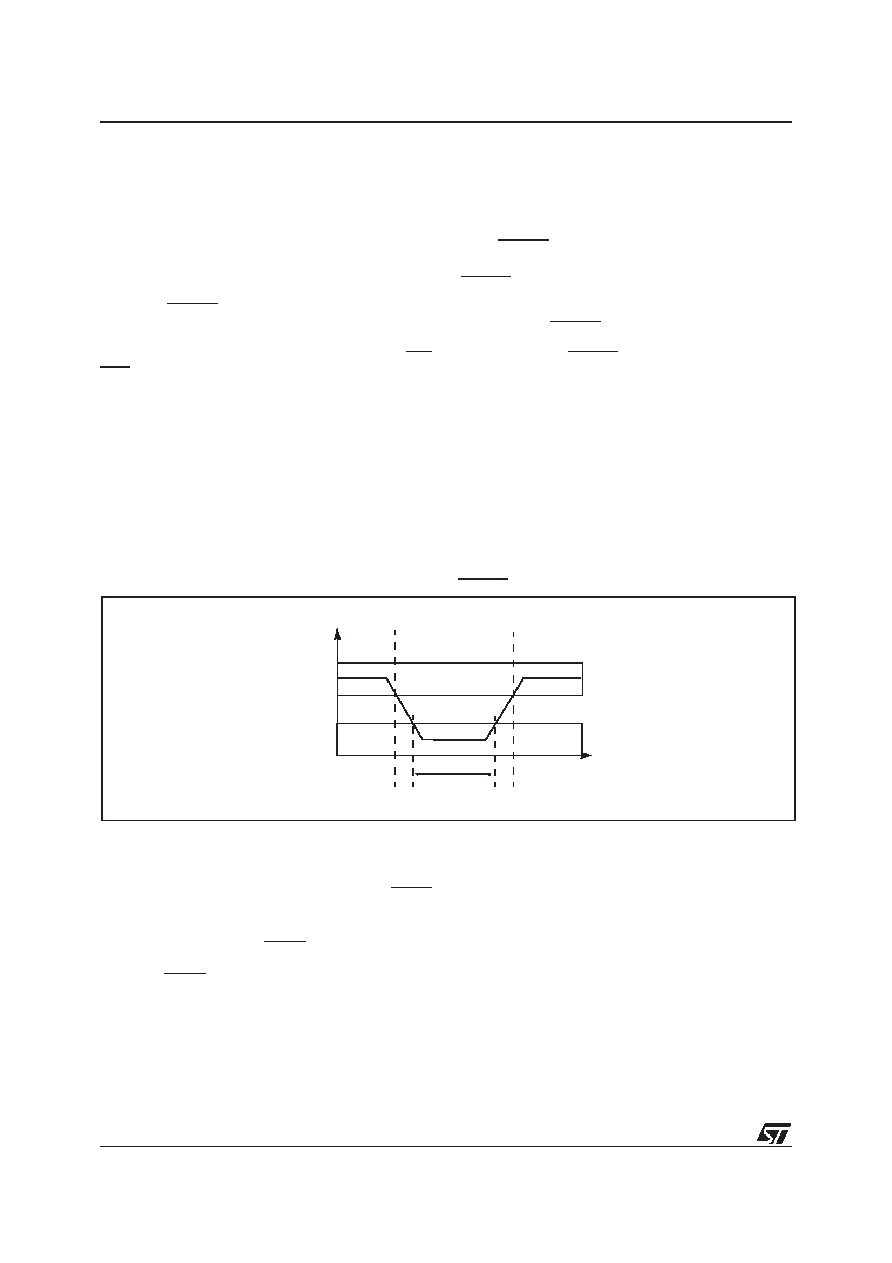
Figure 42. Recommended Signal to be Applied on RESET Pin
6.7 EXTERNAL STOP MODE
On ST9 devices provided with an external STOP
pin, the Reset/Stop Manager can also stop all os-
cillators without resetting the device.
To enter Stop Mode, the STOP pin must be forced
to “0” for a minimum of 4 system clock cycles;
while the STOP pin is kept at “0”, the MCU will re-
main in Stop Mode and all context information will
be preserved. During this condition the internal
clock will be frozen in the high state.
When the pin is forced back to “1”, the MCU
resumes execution of the user program after a de-
lay of 255 CLOCK2 periods.
On exiting from Stop mode an interrupt is generat-
ed and the EX_STP bit in CLK_FLAG will be set,
to indicate to the user program that the machine is
exiting from Stop mode.
VRESET
VDD
0.7 VDD
0.3 VDD
20
s
Minimum
9
相关PDF资料 |
PDF描述 |
|---|---|
| ST92186B3BK | 16-BIT, MROM, 24 MHz, MICROCONTROLLER, PDIP32 |
| ST92195B2T1/XXX | 16-BIT, MROM, 24 MHz, MICROCONTROLLER, PQFP64 |
| ST92195B3B1/XXX | 16-BIT, MROM, 24 MHz, MICROCONTROLLER, PDIP56 |
| ST92195B4B1/XXX | 16-BIT, MROM, 24 MHz, MICROCONTROLLER, PDIP56 |
| ST92195B5T1/XXX | 16-BIT, MROM, 24 MHz, MICROCONTROLLER, PQFP64 |
相关代理商/技术参数 |
参数描述 |
|---|---|
| ST90158M9T6 | 制造商:未知厂家 制造商全称:未知厂家 功能描述:8-Bit Microcontroller |
| ST90158P9C6 | 制造商:未知厂家 制造商全称:未知厂家 功能描述:8-Bit Microcontroller |
| ST90158-ST90135 | 制造商:STMICROELECTRONICS 制造商全称:STMicroelectronics 功能描述:8/16-BIT MCU FAMILY WITH UP TO 64K ROM/OTP/EPROM AND UP TO 2K RAM |
| ST9016 | 制造商:SEMTECH_ELEC 制造商全称:SEMTECH ELECTRONICS LTD. 功能描述:NPN Silicon Epitaxial Planar Transistor |
| ST9018 | 制造商:SEMTECH_ELEC 制造商全称:SEMTECH ELECTRONICS LTD. 功能描述:NPN Silicon Epitaxial Planar Transistor |
发布紧急采购,3分钟左右您将得到回复。