- 您现在的位置:买卖IC网 > PDF目录69383 > STM32F105VCT6XXX (STMICROELECTRONICS) 32-BIT, FLASH, 72 MHz, RISC MICROCONTROLLER, PQFP100 PDF资料下载
参数资料
| 型号: | STM32F105VCT6XXX |
| 厂商: | STMICROELECTRONICS |
| 元件分类: | 微控制器/微处理器 |
| 英文描述: | 32-BIT, FLASH, 72 MHz, RISC MICROCONTROLLER, PQFP100 |
| 封装: | 14 X 14 MM, ROHS COMPLIANT, LQFP-100 |
| 文件页数: | 22/95页 |
| 文件大小: | 1007K |
| 代理商: | STM32F105VCT6XXX |
第1页第2页第3页第4页第5页第6页第7页第8页第9页第10页第11页第12页第13页第14页第15页第16页第17页第18页第19页第20页第21页当前第22页第23页第24页第25页第26页第27页第28页第29页第30页第31页第32页第33页第34页第35页第36页第37页第38页第39页第40页第41页第42页第43页第44页第45页第46页第47页第48页第49页第50页第51页第52页第53页第54页第55页第56页第57页第58页第59页第60页第61页第62页第63页第64页第65页第66页第67页第68页第69页第70页第71页第72页第73页第74页第75页第76页第77页第78页第79页第80页第81页第82页第83页第84页第85页第86页第87页第88页第89页第90页第91页第92页第93页第94页第95页
STM32F105xx, STM32F107xx
Pinouts and pin description
Doc ID 15274 Rev 4
29/95
97
-
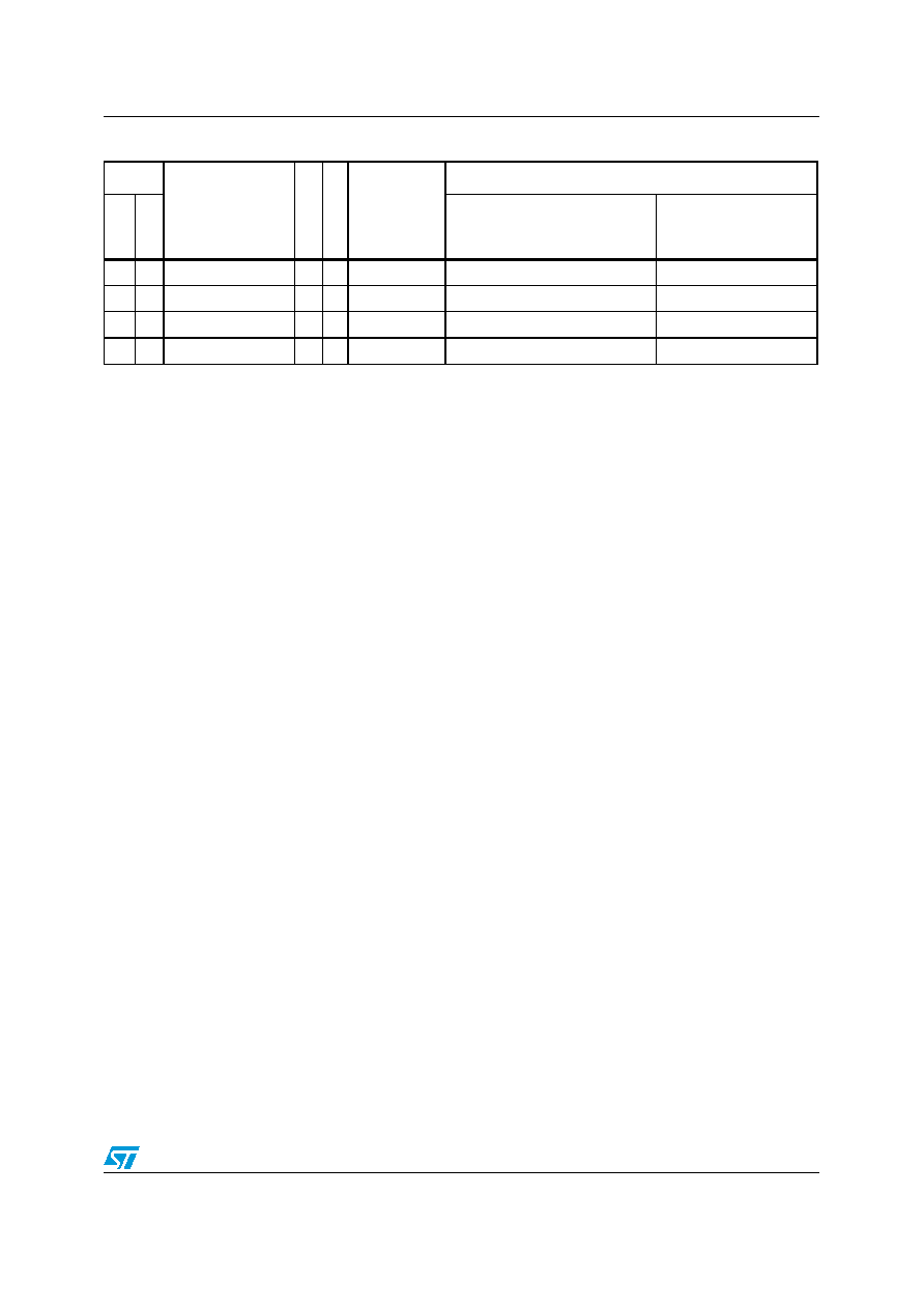
PE0
I/O FT
PE0
TIM4_ETR
98
-
PE1
I/O FT
PE1
99
63
VSS_3
SVSS_3
100 64
VDD_3
SVDD_3
1. I = input, O = output, S = supply.
2. FT = 5 V tolerant. All I/Os are VDD capable.
3. Function availability depends on the chosen device.
4. If several peripherals share the same I/O pin, to avoid conflict between these alternate functions only one peripheral should
be enabled at a time through the peripheral clock enable bit (in the corresponding RCC peripheral clock enable register).
5. PC13, PC14 and PC15 are supplied through the power switch. Since the switch only sinks a limited amount of current
(3 mA), the use of GPIOs PC13 to PC15 in output mode is limited: the speed should not exceed 2 MHz with a maximum
load of 30 pF and these IOs must not be used as a current source (e.g. to drive an LED).
6. Main function after the first backup domain power-up. Later on, it depends on the contents of the Backup registers even
after reset (because these registers are not reset by the main reset). For details on how to manage these IOs, refer to the
Battery backup domain and BKP register description sections in the STM32F10xxx reference manual, available from the
STMicroelectronics website: www.st.com.
7. This alternate function can be remapped by software to some other port pins (if available on the used package). For more
details, refer to the Alternate function I/O and debug configuration section in the STM32F10xxx reference manual,
available from the STMicroelectronics website: www.st.com.
8. For the LQFP64 package, the pins number 5 and 6 are configured as OSC_IN/OSC_OUT after reset, however the
functionality of PD0 and PD1 can be remapped by software on these pins. For the LQFP100 package, PD0 and PD1 are
available by default, so there is no need for remapping. For more details, refer to Alternate function I/O and debug
configuration section in the STM32F10xxx reference manual.
Table 5.
Pin definitions (continued)
Pins
Pin name
Ty
p
e
(1
)
I/
O
le
vel
(2)
Main
function(3)
(after reset)
Alternate functions(4)
LQ
FP10
0
LQ
FP64
Default
Remap
相关PDF资料 |
PDF描述 |
|---|---|
| STM32F105VBT6TR | 32-BIT, FLASH, 72 MHz, RISC MICROCONTROLLER, PQFP100 |
| STM32F105VCT7TR | 32-BIT, FLASH, 72 MHz, RISC MICROCONTROLLER, PQFP100 |
| STM32F105V8T6XXX | 32-BIT, FLASH, 72 MHz, RISC MICROCONTROLLER, PQFP100 |
| STM32F105VCT6TR | 32-BIT, FLASH, 72 MHz, RISC MICROCONTROLLER, PQFP100 |
| STM32F107RBT6XXX | 32-BIT, FLASH, 72 MHz, RISC MICROCONTROLLER, PQFP64 |
相关代理商/技术参数 |
参数描述 |
|---|---|
| STM32F105VCT7 | 功能描述:ARM微控制器 - MCU 32-Bit Cortex 64Kb Connectivity Line RoHS:否 制造商:STMicroelectronics 核心:ARM Cortex M4F 处理器系列:STM32F373xx 数据总线宽度:32 bit 最大时钟频率:72 MHz 程序存储器大小:256 KB 数据 RAM 大小:32 KB 片上 ADC:Yes 工作电源电压:1.65 V to 3.6 V, 2 V to 3.6 V, 2.2 V to 3.6 V 工作温度范围:- 40 C to + 85 C 封装 / 箱体:LQFP-48 安装风格:SMD/SMT |
| STM32F107RB | 制造商:STMicroelectronics 功能描述: |
| STM32F107RBT6 | 功能描述:ARM微控制器 - MCU 32BIT Cortex 64/25 CONNECTIVITY LINE M3 RoHS:否 制造商:STMicroelectronics 核心:ARM Cortex M4F 处理器系列:STM32F373xx 数据总线宽度:32 bit 最大时钟频率:72 MHz 程序存储器大小:256 KB 数据 RAM 大小:32 KB 片上 ADC:Yes 工作电源电压:1.65 V to 3.6 V, 2 V to 3.6 V, 2.2 V to 3.6 V 工作温度范围:- 40 C to + 85 C 封装 / 箱体:LQFP-48 安装风格:SMD/SMT |
| STM32F107RCT6 | 功能描述:ARM微控制器 - MCU 32BIT Cortex 64/25 CONNECTIVITY LINE M3 RoHS:否 制造商:STMicroelectronics 核心:ARM Cortex M4F 处理器系列:STM32F373xx 数据总线宽度:32 bit 最大时钟频率:72 MHz 程序存储器大小:256 KB 数据 RAM 大小:32 KB 片上 ADC:Yes 工作电源电压:1.65 V to 3.6 V, 2 V to 3.6 V, 2.2 V to 3.6 V 工作温度范围:- 40 C to + 85 C 封装 / 箱体:LQFP-48 安装风格:SMD/SMT |
| STM32F107RCT6TR | 功能描述:ARM微控制器 - MCU 32BIT CORTEX M3 256K Flash 6KB RAM RoHS:否 制造商:STMicroelectronics 核心:ARM Cortex M4F 处理器系列:STM32F373xx 数据总线宽度:32 bit 最大时钟频率:72 MHz 程序存储器大小:256 KB 数据 RAM 大小:32 KB 片上 ADC:Yes 工作电源电压:1.65 V to 3.6 V, 2 V to 3.6 V, 2.2 V to 3.6 V 工作温度范围:- 40 C to + 85 C 封装 / 箱体:LQFP-48 安装风格:SMD/SMT |
发布紧急采购,3分钟左右您将得到回复。