- 您现在的位置:买卖IC网 > PDF目录98149 > SX28AC/SSU 2 CHANNEL(S), I2C BUS CONTROLLER, PDSO28 PDF资料下载
参数资料
| 型号: | SX28AC/SSU |
| 元件分类: | 微控制器/微处理器 |
| 英文描述: | 2 CHANNEL(S), I2C BUS CONTROLLER, PDSO28 |
| 封装: | GREEN, PLASTIC, SSOP-28 |
| 文件页数: | 13/48页 |
| 文件大小: | 772K |
| 代理商: | SX28AC/SSU |
第1页第2页第3页第4页第5页第6页第7页第8页第9页第10页第11页第12页当前第13页第14页第15页第16页第17页第18页第19页第20页第21页第22页第23页第24页第25页第26页第27页第28页第29页第30页第31页第32页第33页第34页第35页第36页第37页第38页第39页第40页第41页第42页第43页第44页第45页第46页第47页第48页
2005 Ubicom, Inc. All rights reserved.
- 20 -
www.ubicom.com
SX20AC/SX28AC
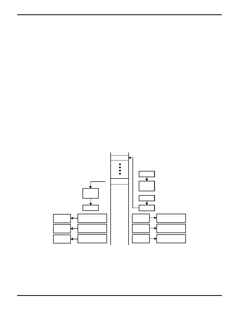
All interrupts are global in nature; that is, no interrupt has
priority over another. Interrupts are handled sequentially.
Figure 8-2 shows the interrupt processing sequence.
Once an interrupt is acknowledged, all subsequent global
interrupts are disabled until return from servicing the cur-
rent interrupt. The PC is pushed onto the single level
interrupt stack, and the contents of the FSR, STATUS,
and W registers are saved in their corresponding shadow
registers. The status bits PA0, PA1, and PA2 bits are
cleared after the STATUS register has been saved in its
shadow register. The interrupt logic has its own single-
level stack and is not part of the CALL subroutine stack.
The vector for the interrupt service routine is address 0.
Once in the interrupt service routine, the user program
must check all external interrupt pending bits (contained
in the WKPND_B register) to determine the source of the
interrupt. The interrupt service routine should clear the
corresponding interrupt pending bit. If both internal and
external interrupts are enabled, the user program may
also need to read the contents of RTCC to determine any
recent RTCC rollover. This is needed since there is no
interrupt pending bit associated with the RTCC rollover.
Normally it is a requirement for the user program to pro-
cess every interrupt without missing any. To ensure this,
the longest path through the interrupt routine must take
less time than the shortest possible delay between inter-
rupts.
If an external interrupt occurs during the interrupt routine,
the pending register will be updated but the trigger will be
ignored unless interrupts are disabled at the beginning of
the interrupt routine and enabled again at the end. This
also requires that the new interrupt does not occur before
interrupts are disabled in the interrupt routine. If there is a
possibility of additional interrupts occurring before they
can be disabled, the device will miss those interrupt trig-
gers. In other words, using more than one interrupt, such
as multiple external interrupts or both RTCC and external
interrupts, can result in missed or, at best, jittery interrupt
handling should one occur during the processing of
another. When handling external interrupts, the interrupt
routine should clear at least one pending register bit. The
bit that is cleared should represent the interrupt being
handled in order for the next interrupt to trigger.
Upon return from the interrupt service routine, the con-
tents of PC, FSR, STATUS, and W registers are restored
from their corresponding shadow registers. The interrupt
service routine should end with instructions such as RETI
and RETIW. RETI pops the interrupt stack and the spe-
cial shadow registers used for storing W, STATUS, and
FSR (preserved during interrupt handling). RETIW
behaves like RETI but also adds W to RTCC. The inter-
rupt return instruction enables the global interrupts.
Figure 8-2. Interrupt Processing
Interrupt
PC
RETI
PC
W
Register
000h
Address 000h
Program
Memory
Interrupt
Service
Routine
STATUS
Register
FSR
Register
W
Shadow Register
STATUS
Shadow Register
FSR
Shadow Register
W
Register
STATUS
Register
FSR
Register
W
Shadow Register
STATUS
Shadow Register
FSR
Shadow Register
Stack
Interrupt
Stack
Note: The interrupt logic has its own single-level
stack and is not part of the CALL subroutine stack.
相关PDF资料 |
PDF描述 |
|---|---|
| SY100EP11UZITR | 100E SERIES, LOW SKEW CLOCK DRIVER, 2 TRUE OUTPUT(S), 0 INVERTED OUTPUT(S), PDSO8 |
| SY100EP195VTCTR | ACTIVE DELAY LINE, COMPLEMENTARY OUTPUT, PQFP32 |
| SY100EP195VTG | ACTIVE DELAY LINE, COMPLEMENTARY OUTPUT, PQFP32 |
| SY100EP196VTCTR | ACTIVE DELAY LINE, COMPLEMENTARY OUTPUT, PQFP32 |
| SY100EP196VTC | ACTIVE DELAY LINE, COMPLEMENTARY OUTPUT, PQFP32 |
相关代理商/技术参数 |
参数描述 |
|---|---|
| SX28AD100-I/DP | 制造商:未知厂家 制造商全称:未知厂家 功能描述:Configurable Communications Controllers with EE/Flash Program Memory, In-System Programming Capability and On-Chip Debug |
| SX28AD100-I/PQ | 制造商:未知厂家 制造商全称:未知厂家 功能描述:Configurable Communications Controllers with EE/Flash Program Memory, In-System Programming Capability and On-Chip Debug |
| SX28AD100-I/SO | 制造商:未知厂家 制造商全称:未知厂家 功能描述:Configurable Communications Controllers with EE/Flash Program Memory, In-System Programming Capability and On-Chip Debug |
| SX28AD100-I/SS | 制造商:未知厂家 制造商全称:未知厂家 功能描述:Configurable Communications Controllers with EE/Flash Program Memory, In-System Programming Capability and On-Chip Debug |
| SX28AD100-I/TQ | 制造商:未知厂家 制造商全称:未知厂家 功能描述:Configurable Communications Controllers with EE/Flash Program Memory, In-System Programming Capability and On-Chip Debug |
发布紧急采购,3分钟左右您将得到回复。