- 您现在的位置:买卖IC网 > PDF目录383915 > TC1307 (Microchip Technology Inc.) Four-Channel CMOS LDO with Select Mode, Shutdown and Independent Reset PDF资料下载
参数资料
| 型号: | TC1307 |
| 厂商: | Microchip Technology Inc. |
| 英文描述: | Four-Channel CMOS LDO with Select Mode, Shutdown and Independent Reset |
| 中文描述: | 四通道CMOS低压降稳压器的选择模式,关机和独立复位 |
| 文件页数: | 2/28页 |
| 文件大小: | 553K |
| 代理商: | TC1307 |
第1页当前第2页第3页第4页第5页第6页第7页第8页第9页第10页第11页第12页第13页第14页第15页第16页第17页第18页第19页第20页第21页第22页第23页第24页第25页第26页第27页第28页
TC1307
DS21702A-page 2
2002 Microchip Technology Inc.
1.0
ELECTRICAL
CHARACTERISTICS
1.1
Maximum Ratings*
V
DD
..............................................................................
6.5V
All inputs and outputs w.r.t. ....... ...V
IN
+ 0.3V to -0.3V
Output Short Circuit Current ...... ...............continuous
Storage temperature.................... .... -65°C to +150°C
Operating Junction Temperature,
T
J
..................................................-40°C < T
J
< +150°C
Maximum Junction Temperature, T
J
..................150°C
ESD protection on all pins...................................
≥
4 kV
*Notice:
Stresses above those listed under “Maximum
Ratings” may cause permanent damage to the device.
This is a stress rating only and functional operation of
the device at those or any other conditions above those
indicated in the operational listings of this specification
is not implied. Exposure to maximum rating conditions
for extended periods may affect device reliability.
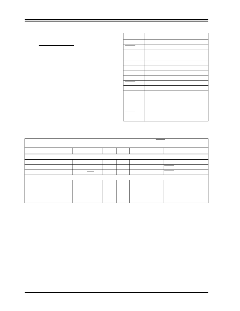
PIN FUNCTION TABLE
ELECTRICAL CHARACTERISTICS
Name
Function
V
DET
SHDN1
Voltage Detect Input
Shutdown for V
OUT1
Input for setting V
OUT1
and V
OUT2.
Input Voltage Connection
SELECT12
V
IN
V
IN
GND
Input Voltage Connection
Ground connection
SHDN3
Shutdown for V
OUT3
Input Voltage Connection
V
IN
SHDN4
Shutdown for V
OUT4
Input for setting V
OUT3
and V
OUT4.
LDO4 Output
SELECT34
V
OUT4
V
OUT3
V
OUT2
V
OUT1
SHDN2
LDO3 Output
LDO2 Output
LDO1 Output
Shutdown for V
OUT2
Reset Output
RESET
Unless otherwise specified, all limits are established for V
IN
= V
R
+1, I
L
= 100 μA, C
L
= 3.3 μF, SHDN > V
IH
, T
A
= 25°C.
Boldface
type specifications apply for junction temperatures, T
J
(
Note 9
) of -40°C to +125°C.
Parameter
Sym
Min
Typ
Max
Units
Conditions
Input Characteristics:
Input Operating Voltage
V
IN
I
IN
2.7
—
6.0
V
Note 1
Input Quiescent Current
—
220
370
μA
SHDN = V
IH
, I
L
= 0
SHDN = 0V
Input Shutdown Current
I
IN_SHDN
—
0.1
0.5
μA
Output Characteristics:
Maximum Output Current
I
OUT_MAX
I
OUT_SC
150
—
mA
Output Short Circuit Current
(Average)
—
360
—
mA
V
OUT
= 0V
Voltage Regulation
LDO1/LDO2/LDO3/LDO4
Note 1:
The minimum V
IN
must meet two conditions
:
V
IN
≥
2.7
V
and V
IN
≥
(V
R
+ 2.5%)
+
V
DROPOUT
.
2:
V
R
is the nominal regulator output voltage. For example: V
R
= 1.8V, 2.5V, 2.8V or 3.0V.
3:
TCV
OUT
= (V
OUT-HIGH
- V
OUT-LOW
)
*
10
6
/ (
V
R
*
Temperature),
V
OUT-HIGH
=
Highest voltage measured over the tempera-
ture range. V
OUT-LOW
= Lowest voltage measured over the temperature range.
4:
Load regulation is measured at a constant junction temperature using low duty cycle pulse testing. Load regulation is
tested over a load range from 1mA to the maximum specified output current. Changes in output voltage due to heating
effects are determined using thermal regulation specification TCV
OUT
.
5:
Thermal regulation is defined as the change in output voltage at a time t after a change in power dissipation is applied.
Specifications are for a current pulse equal to I
LMAX
at V
IN
= 6.0V for t = 10 msec.
6:
Dropout voltage is defined as the input to output differential at which the output voltage drops 2% below its nominal value
with a 1V differential applied.
7:
The maximum allowable power dissipation is a function of ambient temperature, the maximum allowable junction temper-
ature and the thermal resistance from junction to air. (i.e. T
A
, T
J
,
θ
JA
). Exceeding the maximum allowable power dissipa-
tion will cause the device operating junction temperature to exceed the maximum 150°C rating. Sustained junction
temperatures above 150°C can impact the device reliability.
8:
V
TH-MIN
= 2.55V and V
TH-MAX
= 2.70V.
9:
The Junction temperature is approximated by soaking the device under test at an ambient temperature equal to the
desired Junction temperature. The test time is small enough such that the rise in the Junction temperature over the Ambi-
ent temperature is not significant.
V
OUT
V
R
-2.5%
V
R
±0.5
V
R
+2.5%
V
Note 2
相关PDF资料 |
PDF描述 |
|---|---|
| TC1313-CL0EMFTR | 500 mA Synchronous Buck Regulator, + 300 mA LDO |
| TC1313-CL0EUN | 500 mA Synchronous Buck Regulator, + 300 mA LDO |
| TC1313-CL0EUNTR | 500 mA Synchronous Buck Regulator, + 300 mA LDO |
| TC1313-CL1EMF | 500 mA Synchronous Buck Regulator, + 300 mA LDO |
| TC1313-CL1EMFTR | 500 mA Synchronous Buck Regulator, + 300 mA LDO |
相关代理商/技术参数 |
参数描述 |
|---|---|
| TC1307R-XYVQRTR | 功能描述:低压差稳压器 - LDO Dual LDO w/ Sdn RoHS:否 制造商:Texas Instruments 最大输入电压:36 V 输出电压:1.4 V to 20.5 V 回动电压(最大值):307 mV 输出电流:1 A 负载调节:0.3 % 输出端数量: 输出类型:Fixed 最大工作温度:+ 125 C 安装风格:SMD/SMT 封装 / 箱体:VQFN-20 |
| TC130AW10 | 制造商:Panduit Corp 功能描述: |
| TC130EI10 | 功能描述:电线导管 T130 Power Rated Multi-Channel Raceway C RoHS:否 制造商:Panduit 类型:Slotted SideWall Open finger design wiring cut 材料:Polypropylene 颜色:Light Gray 大小: 最大光束直径: 抗拉强度: 外部导管宽度:25 mm 外部导管高度:25 mm |
| TC130EI6 | 功能描述:电线导管 T130 Power Rated Multi-Channel Raceway C RoHS:否 制造商:Panduit 类型:Slotted SideWall Open finger design wiring cut 材料:Polypropylene 颜色:Light Gray 大小: 最大光束直径: 抗拉强度: 外部导管宽度:25 mm 外部导管高度:25 mm |
| TC130EI8 | 功能描述:电线导管 T130 Power Rated Multi-Channel Raceway C RoHS:否 制造商:Panduit 类型:Slotted SideWall Open finger design wiring cut 材料:Polypropylene 颜色:Light Gray 大小: 最大光束直径: 抗拉强度: 外部导管宽度:25 mm 外部导管高度:25 mm |
发布紧急采购,3分钟左右您将得到回复。