参数资料
| 型号: | TC530CPJ |
| 厂商: | Microchip Technology |
| 文件页数: | 28/28页 |
| 文件大小: | 0K |
| 描述: | IC DATA ACQ SUBSYSTEM 28DIP |
| 标准包装: | 15 |
| 类型: | 数据采集系统(DAS) |
| 分辨率(位): | 17 b |
| 采样率(每秒): | 6.5 |
| 数据接口: | 串行 |
| 电压电源: | 单电源 |
| 电源电压: | 4.5 V ~ 5.5 V |
| 工作温度: | 0°C ~ 70°C |
| 安装类型: | 通孔 |
| 封装/外壳: | 28-DIP(0.300",7.62mm) |
| 供应商设备封装: | 28-DIP |
| 包装: | 管件 |
| 其它名称: | Q1000542A |
第1页第2页第3页第4页第5页第6页第7页第8页第9页第10页第11页第12页第13页第14页第15页第16页第17页第18页第19页第20页第21页第22页第23页第24页第25页第26页第27页当前第28页
2007 Microchip Technology Inc.
DS21433C-page 9
TC530/TC534
4.0
DETAILED DESCRIPTION
4.1
Dual Slope Integrating Converter
The TC530/TC534 dual slope converter operates by
integrating the input signal for a fixed time period, then
applying an opposite polarity reference voltage while
timing the period (counting clocks pulses) for the
integrator output to cross 0V (deintegrating). The
resulting count is read as conversion data.
A simple mathematical expression that describes dual
slope conversion is:
EQUATION 4-1:
EQUATION 4-2:
from which:
EQUATION 4-3:
And therefore:
EQUATION 4-4:
Inspection of Equation 4-4 shows dual slope converter
accuracy is unrelated to integrating resistor and
capacitor values, as long as they are stable throughout
the measurement cycle. This measurement technique
is inherently ratiometric (i.e., the ratio between the TINT
and TDEINT times is equal to the ratio between VIN and
VREF).
Another inherent benefit is noise immunity. Input noise
spikes are integrated, or averaged to zero, during the
integration period. The integrating converter has a noise
immunity with an attenuation rate of at least -20 dB per
decade. Interference signals with frequencies at integral
multiples of the integration period are, for the most part,
completely removed. For this reason, the integration
period of the converter is often established to reject
50/60 Hz line noise. The ability to reject such noise is
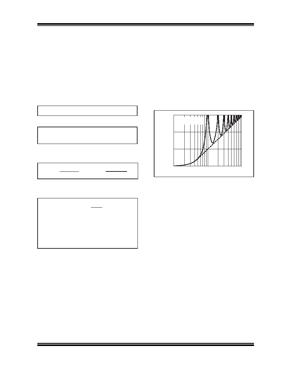
shown by the plot of Figure 4-1.
In addition to the two phases required for dual slope
measurement (Integrate
and
De-integrate), the
TC530/TC534 performs two additional adjustments to
minimize measurement error due to system offset volt-
ages. The resulting four internal operations (conver-
sion phases) performed each measurement cycle are:
Auto Zero (AZ), Integrator Output Zero (IZ), Input
Integrate (INT) and Reference De-integrate (DINT).
The AZ and IZ phases compensate for system offset
errors and the INT and DINT phases perform the actual
A/D conversion.
FIGURE 4-1:
Integrating Converter
Normal Mode Rejection.
4.2
Auto Zero Phase (AZ)
This phase compensates for errors due to buffer,
integrator and comparator offset voltages. During this
phase,
an
internal
feedback
loop
forces
a
compensating error voltage on auto zero capacitor
(CAZ). The duration of the AZ phase is programmable
via the serial port (see Section 5.1.1 “AZ and INT
Phase Duration”, AZ and INT Phase Duration).
Integrate Voltage = De-integrate Voltage
1
RINTCINT
------------------------ T
INT
0
∫
VIN T
()dT
1
RINTCINT
------------------------ T
DEINT
0
∫
VREF
=
(VIN)
(RINT)(CINT)
[ (TINT) =(V
REF)
]
(RINT)(CINT)
[ (TDEINT) ]
VIN = VREF
[ ]
TINT
TDEINT
Where:
VREF
=
Reference Voltage
TINT
=
Integrate Time
TDEINT
=
Reference Voltage De-integrate
Time
30
20
10
0
0.1/T
1/T
10/T
Input Frequency
Normal
Mode
Rejection
(dB)
T = Measurement
Period
相关PDF资料 |
PDF描述 |
|---|---|
| MS3108A20-33P | CONN PLUG 11POS RT ANG W/PINS |
| M83723/83W1814N | CONN RCPT 14POS WALL MT W/PINS |
| MAX180AEPL+ | IC DAS 12BIT 100KSPS 40-DIP |
| M83723/83R1814N | CONN RCPT 14POS WALL MT W/PINS |
| MS27473E22B55PD | CONN PLUG 55POS STRAIGHT W/PINS |
相关代理商/技术参数 |
参数描述 |
|---|---|
| TC531000AP-F711 | 制造商:Toshiba America Electronic Components 功能描述:531000AP-F711 |
| TC531001 | 制造商:TOSHIBA 制造商全称:Toshiba Semiconductor 功能描述:1M BIT (128K WORD x 8 BIT) CMOS MASK ROM |
| TC531001CF | 制造商:Toshiba America Electronic Components 功能描述: |
| TC531001CF-12 | 制造商:TOSHIBA 制造商全称:Toshiba Semiconductor 功能描述:1M BIT (128K WORD x 8 BIT) CMOS MASK ROM |
| TC531001CF-15 | 制造商:TOSHIBA 制造商全称:Toshiba Semiconductor 功能描述:1M BIT (128K WORD x 8 BIT) CMOS MASK ROM |
发布紧急采购,3分钟左右您将得到回复。