- 您现在的位置:买卖IC网 > PDF目录98181 > TC820CLW 1-CH DUAL-SLOPE ADC, PQCC44 PDF资料下载
参数资料
| 型号: | TC820CLW |
| 元件分类: | ADC |
| 英文描述: | 1-CH DUAL-SLOPE ADC, PQCC44 |
| 封装: | PLASTIC, LCC-44 |
| 文件页数: | 9/28页 |
| 文件大小: | 616K |
| 代理商: | TC820CLW |
第1页第2页第3页第4页第5页第6页第7页第8页当前第9页第10页第11页第12页第13页第14页第15页第16页第17页第18页第19页第20页第21页第22页第23页第24页第25页第26页第27页第28页
2002 Microchip Technology Inc.
DS21476B-page 17
TC820
5.0
TYPICAL APPLICATIONS
5.1
Power Supplies
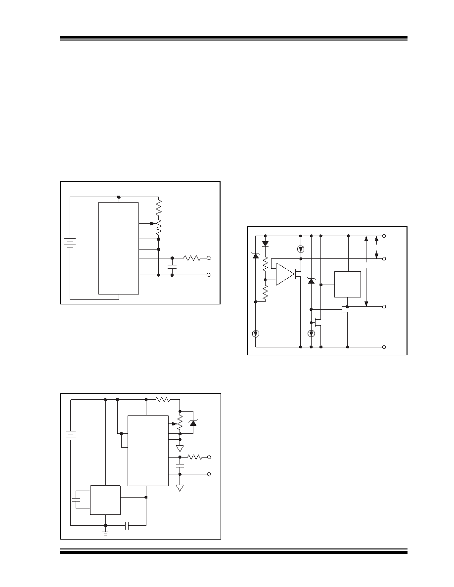
The TC820 is designed to operate from a single power
supply such as a 9V battery (Figure 5-1). The converter
will operate over a range of 7V to 15V. For battery oper-
ation, analog common (COM) provides a Common
mode bias voltage (see analog common discussion in
the theory of operation section). However, measure-
ments cannot be referenced to battery ground. To do so
will exceed the Negative Common mode voltage limit.
FIGURE 5-1:
POWERING THE TC820
FROM A SINGLE 9V
BATTERY
A battery with voltage between 3.5V and 7V can be
used to power the TC820, when used with a voltage
doubler, as shown in Figure 5-2. The voltage doubler
uses the TC7660 and two external capacitors. With this
configuration, measurements can be referenced either
to analog common or to battery ground.
FIGURE 5-2:
POWERING THE TC820
FROM A LOW VOLTAGE
BATTERY
5.2
Digital Ground (DGND)
Digital ground is generated from an internal zener
diode (Figure 5-3). The voltage between VDD and
DGND is the internal supply voltage for the digital sec-
tion of the TC820. DGND will sink a minimum of 3mA.
DGND establishes the low logic level reference for the
TC820 mode select inputs, and for the frequency and
logic probe inputs. The DGND pin can be used as the
negative supply for external logic gates, such as the
logic probe buffers. To ensure correct counter opera-
tion at high frequency, connect a 1
F capacitor from
DGND to VDD.
DGND also provides the drive voltage for the LCD. The
TC820 40-pin package internally connects the LCD
VDISP pin to DGND, and provides an LCD drive voltage
of about 5VP-P. In the 44-pin package, connecting the
VDISP pin to DGND will provide a 5V LCD drive voltage.
FIGURE 5-3:
DGND AND COM
OUTPUTS
5.3
Digital Input Logic Levels
Logic levels for the TC820 digital inputs are referenced
to VDD and DGND. The high level threshold is
VDD – 1.5V, and the low logic level is DGND + 1.5V. In
most cases, digital inputs will be connected directly to
VDD with a mechanical switch. CMOS gates can also
be used to control the logic inputs, as shown in the logic
probe inputs section.
5.4
Clock Oscillator
The TC820 oscillator can be controlled with either a
crystal, or with an inexpensive resistor capacitor com-
bination. The crystal circuit, shown in Figure 5-4, is rec-
ommended when high accuracy is required in the
Frequency Counter mode. The 40kHz crystal is a stan-
dard frequency for ultrasonic alarms, and will provide a
1-second time-base for the counter or 2.5 analog-to-
digital conversions per second. Consult the crystal
manufacturer for detailed applications information.
TC820
VIN
VREF-
VDD
VREF+
COM
VIN+
VIN-
VSS
+
–
9V
+
–
VDD
VSS
VREF+
VREF-
TC820
3.5V to 6V
TC7660
VIN+
VIN-
+
–
VIN
10F
3
4
2
8
5
10F
+
COM
+
–
12A
P
TC820
Logic
Section
5V
3.2V
N
VDD
VSS
COM
DGND
相关PDF资料 |
PDF描述 |
|---|---|
| TC820CPL | 1-CH DUAL-SLOPE ADC, PDIP40 |
| TC820CLW | DUAL-SLOPE ADC, PARALLEL ACCESS, PQCC44 |
| TC820CPL | DUAL-SLOPE ADC, PARALLEL ACCESS, PDIP40 |
| TC821CKW | CONVERTER SUBSYSTEM ADC, PARALLEL ACCESS, PQFP44 |
| TC821CLW | CONVERTER SUBSYSTEM ADC, PARALLEL ACCESS, PQCC44 |
相关代理商/技术参数 |
参数描述 |
|---|---|
| TC820CLW713 | 功能描述:LCD 驱动器 3-3/4 A/D Converter RoHS:否 制造商:Maxim Integrated 数位数量:4.5 片段数量:30 最大时钟频率:19 KHz 工作电源电压:3 V to 3.6 V 最大工作温度:+ 85 C 最小工作温度:- 20 C 封装 / 箱体:PDIP-40 封装:Tube |
| TC820CPL | 功能描述:LCD 驱动器 3-3/4 A/D Converter RoHS:否 制造商:Maxim Integrated 数位数量:4.5 片段数量:30 最大时钟频率:19 KHz 工作电源电压:3 V to 3.6 V 最大工作温度:+ 85 C 最小工作温度:- 20 C 封装 / 箱体:PDIP-40 封装:Tube |
| TC8-20S2405R | 制造商:TRUMPOWER 制造商全称:Tumbler Technologies + TRUMPower 功能描述:DC/DC CONVERTERS 2:1 Input, 12.5 to 20 Watt |
| TC8-20S4805R | 制造商:TRUMPOWER 制造商全称:Tumbler Technologies + TRUMPower 功能描述:DC/DC CONVERTERS 2:1 Input, 12.5 to 20 Watt |
| TC-821-SC | 制造商:Thomas & Betts 功能描述:Cable Accessories Thin Wall Conduit Fitting Zinc Die Cast |
发布紧急采购,3分钟左右您将得到回复。