- 您现在的位置:买卖IC网 > PDF目录98204 > TDA9116 (STMICROELECTRONICS) HORIZ/VERT DEFLECTION IC, PDIP32 PDF资料下载
参数资料
| 型号: | TDA9116 |
| 厂商: | STMICROELECTRONICS |
| 元件分类: | 偏转 |
| 英文描述: | HORIZ/VERT DEFLECTION IC, PDIP32 |
| 封装: | SHRINK, PLASTIC, DIP-32 |
| 文件页数: | 5/47页 |
| 文件大小: | 725K |
| 代理商: | TDA9116 |
第1页第2页第3页第4页当前第5页第6页第7页第8页第9页第10页第11页第12页第13页第14页第15页第16页第17页第18页第19页第20页第21页第22页第23页第24页第25页第26页第27页第28页第29页第30页第31页第32页第33页第34页第35页第36页第37页第38页第39页第40页第41页第42页第43页第44页第45页第46页第47页
TDA9116
13/47
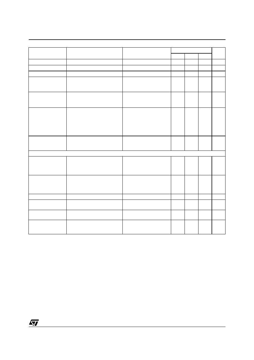
Note 10: Value of acceptable cumulated parasitic load resistance due to humidity, AGC storage capacitor leakage, etc.,
for less than 1% of
Vamp change.
Note 11: The threshold for VVOB is generated internally and routed to VOscF pin. Any DC current on this pin will
influence the value of VVOB.
Note 12: Maximum of deviation from an ideally linear sawtooth ramp at null
SCOR (Sad09 at x0000000b) and null CCOR
(Sad0A at x1000000b). The same rate applies to V-drive signal on VOut pin.
Note 13: Maximum
SCOR (Sad09 at x1111111b), null CCOR (Sad0A at x1000000b).
Note 14: Null
SCOR (Sad09 at x0000000b).
Note 15: "tVR" is time from the beginning of vertical ramp of V-drive signal on VOut pin. "TVR" is duration of this ramp, see
chapter TYPICAL OUTPUT WAVEFORMS and Figure 13.
Note 16: VVOamp = VVOT -VVOB
Note 17: The same rate applies to V-drive signal on VOut pin.
Note 18: Informative, not tested on each unit.
tVODis
Sawtooth Discharge time
CVCap=150nF
80
s
fVO(0)
Free-running frequency
CVCap=150nF
100
Hz
fVOCapt
AGC loop capture frequency
CVCap=150nF
50
185
Hz
Sawtooth non-linearity(12)
AGC loop stabilized, (12)
0.5
%
S-correction range
AGC loop stabilized, (13)
tVR=1/4 TVR
(15)
tVR=3/4 TVR
-5
+5
%
C-correction range
AGC loop stabilized, (14)
tVR=1/2 TVR
(15)
CCOR(Sad0A):
x0000000b
x1000000b
x1111111b
-3
0
+3
%
Frequency drift of sawtooth
amplitude(17)(18)
AGC loop stabilized
fVOCapt(min)<fVO<fVOCapt(max)
200
ppm/
Hz
Vertical output drive signal (on pin VOut);VRefO = 8V
Vmid(VOut)
Middle point on VOut sawtooth
VPOS (Sad08):
x0000000b
x1000000b
x1111111b
3.65
3.2
3.5
3.8
3.3
V
Vamp
Amplitude of VOut sawtooth
(peak-to-peak voltage)
VSIZE (Sad07):
x0000000b
x1000000b
x1111111b
3.5
2.25
3.0
3.75
2.5
V
VoffVOut
Level on VOut pin at V-drive "off" I2Cbit
VOutEn at 0
3.8
V
IVOut
Current delivered by VOut out-
put
-5
5
mA
VVEHT
Control input voltage range on
VEHTIn pin
1
VRefO
V
Breathing compensation
VVEHT>VRefO
VVEHT(min)<VVEHT<VRefO
0
2.5
%/V
Symbol
Parameter
Test Conditions
Value
Units
Min.
Typ.
Max.
V
VOdev
D
V
VOamp 16
()
---------------------------------
V
VOS
cor
–
D
V
VO amp
---------------------------------
V
VO C
cor
–
D
V
VO amp
---------------------------------
V
VOamp
D
V
VO amp
f
VO
-----------------------------------------
V
amp
V
amp
V
VEHT
------------------------------------------
相关PDF资料 |
PDF描述 |
|---|---|
| TDA9141N | COLOR SIGNAL DECODER, PDIP32 |
| TDA9170N | SPECIALTY CONSUMER CIRCUIT, PDIP32 |
| TDA9177N | SPECIALTY CONSUMER CIRCUIT, PDIP24 |
| TDA9201 | 1 CHANNEL, VIDEO PREAMPLIFIER, PDIP20 |
| TDA9203A | 3 CHANNEL, VIDEO PREAMPLIFIER, PDIP24 |
相关代理商/技术参数 |
参数描述 |
|---|---|
| TDA9118 | 制造商:PHILIPS 制造商全称:NXP Semiconductors 功能描述:行/场扫描处理电路 |
| TDA9141 | 制造商:PHILIPS 制造商全称:NXP Semiconductors 功能描述:PAL/NTSC/SECAM decoder/sync processor |
| TDA9143 | 制造商:PHILIPS 制造商全称:NXP Semiconductors 功能描述:I2C-bus controlled, alignment-free PAL/NTSC/SECAM decoder/sync processor |
| TDA9144 | 制造商:PHILIPS 制造商全称:NXP Semiconductors 功能描述:I2C-bus controlled, alignment-free PAL/NTSC/SECAM decoder/sync processor with PALplus helper demodulator |
| TDA9150 | 制造商:PHILIPS 制造商全称:NXP Semiconductors 功能描述:Programmable deflection controller |
发布紧急采购,3分钟左右您将得到回复。