- 您现在的位置:买卖IC网 > PDF目录98217 > THS1031IDWG4 (TEXAS INSTRUMENTS INC) 1-CH 10-BIT PROPRIETARY METHOD ADC, PARALLEL ACCESS, PDSO28 PDF资料下载
参数资料
| 型号: | THS1031IDWG4 |
| 厂商: | TEXAS INSTRUMENTS INC |
| 元件分类: | ADC |
| 英文描述: | 1-CH 10-BIT PROPRIETARY METHOD ADC, PARALLEL ACCESS, PDSO28 |
| 封装: | GREEN, PLASTIC, SOIC-28 |
| 文件页数: | 19/41页 |
| 文件大小: | 728K |
| 代理商: | THS1031IDWG4 |
第1页第2页第3页第4页第5页第6页第7页第8页第9页第10页第11页第12页第13页第14页第15页第16页第17页第18页当前第19页第20页第21页第22页第23页第24页第25页第26页第27页第28页第29页第30页第31页第32页第33页第34页第35页第36页第37页第38页第39页第40页第41页
THS1031
3-V TO 5.5-V, 10-BIT, 30 MSPS
CMOS ANALOG-TO-DIGITAL CONVERTER
SLAS242E – NOVEMBER 1999 – REVISED MARCH 2002
26
POST OFFICE BOX 655303
DALLAS, TEXAS 75265
PRINCIPLES OF OPERATION
power management
In power-sensitive applications (such as battery-powered systems) where the THS1031 ADC is not required
to convert continuously, power can be saved between conversion intervals by placing the THS1031 into
power-down mode. This is achieved by setting bit 3 (PWDN) of the control register to 1. In power-down mode,
the device typically consumes less than 1 mW of power in either top/bottom or center-span modes. Power-down
mode is exited by resetting control register bit 3 to 0. On power up, the THS1031 typically requires 5 ms of
wake-up time before valid conversion results are available.
In systems where the ADC must run continuously, but where the clamp is not required, setting control register
bit 6 (CLDIS to 1), which disables only the clamp circuits, can save power.
Disabling the ORG in applications where the ORG output is not required can also reduce power dissipation by
1 mA analog IDD. This is achieved by connecting the REFSENSE pin to AVDD.
output format and digital I/O
While the OE pin is held low, ADC conversion results are output at pins I/O0 (LSB) to I/O9 (MSB). The ADC input
over-range indicator is output at pin OVR. OVR is also disabled when OE is held high.
The default ADC output data format is unsigned binary (output codes 0 to 1023). The output format can be
switched to 2s complement (output codes –512 to 511) by setting control register bit 5 (TWOC) to 1.
writing to the internal registers through the digital I/O bus
Pulling pin OE high disables the I/O and OVR pin output drivers, placing the driver outputs in a high impedance
state. This allows control register data to be loaded into the THS1031 by presenting it on the I/O0 to I/O9 pins
and pulsing the WR pin high to latch the data into the chosen control or DAC register.
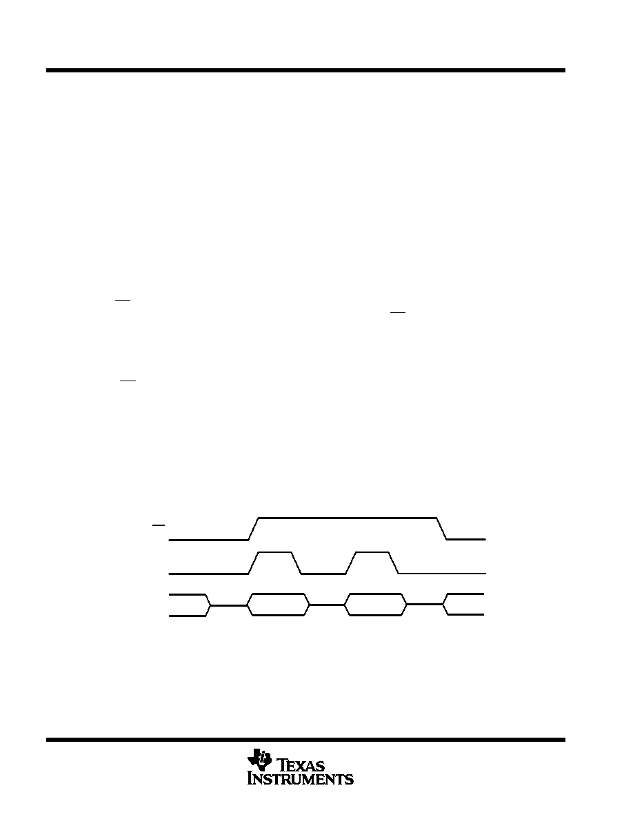
Figure 31 shows an example register write cycle where the clamp DAC code is set to 10F (hex) by writing to
clamp registers 1 and 2 (see the register map in Table 3). Pins I/O0 to I/O7 are driven to the clamp DAC code
lower byte (0F hex) and pins I/08 and I/O9 are both driven to 0 to select clamp register 1 as the data destination.
The clamp low-byte data is then loaded into this register by pulsing WR high. The top 2 bits of the DAC word
are then loaded by driving 01(hex) on pins I/O0 to I/O7 and by driving pin I/O8 to 1 and pin I/O9 to 0 to select
clamp register 2 as the data destination. WR is pulsed a second time to latch this second control word into clamp
register 2. Interface timing parameters are given in Figures 1 and 2.
OE
WR
I/O (0–9)
Output
Input 00F
Input 101
Output
Load 0F Into
REGISTER 0
Load 01 Into
REGISTER 1
Figure 31. Example Register Write Cycle to Clamp DAC Register
相关PDF资料 |
PDF描述 |
|---|---|
| THS1031CDWG4 | 1-CH 10-BIT PROPRIETARY METHOD ADC, PARALLEL ACCESS, PDSO28 |
| THS1031CPWG4 | 1-CH 10-BIT PROPRIETARY METHOD ADC, PARALLEL ACCESS, PDSO28 |
| THS1031CPWR | 1-CH 10-BIT PROPRIETARY METHOD ADC, PARALLEL ACCESS, PDSO28 |
| THS1031IPWLE | 10-CH 10-BIT PROPRIETARY METHOD ADC, PARALLEL ACCESS, PDSO28 |
| THS1031CPWLE | 10-CH 10-BIT PROPRIETARY METHOD ADC, PARALLEL ACCESS, PDSO28 |
相关代理商/技术参数 |
参数描述 |
|---|---|
| THS1031IDWR | 功能描述:模数转换器 - ADC 10-Bit 30 MSPS 1-Ch RoHS:否 制造商:Texas Instruments 通道数量:2 结构:Sigma-Delta 转换速率:125 SPs to 8 KSPs 分辨率:24 bit 输入类型:Differential 信噪比:107 dB 接口类型:SPI 工作电源电压:1.7 V to 3.6 V, 2.7 V to 5.25 V 最大工作温度:+ 85 C 安装风格:SMD/SMT 封装 / 箱体:VQFN-32 |
| THS1031IDWRG4 | 功能描述:模数转换器 - ADC 10-Bit 30 MSPS 1-Ch RoHS:否 制造商:Texas Instruments 通道数量:2 结构:Sigma-Delta 转换速率:125 SPs to 8 KSPs 分辨率:24 bit 输入类型:Differential 信噪比:107 dB 接口类型:SPI 工作电源电压:1.7 V to 3.6 V, 2.7 V to 5.25 V 最大工作温度:+ 85 C 安装风格:SMD/SMT 封装 / 箱体:VQFN-32 |
| THS1031IPW | 功能描述:模数转换器 - ADC _ RoHS:否 制造商:Texas Instruments 通道数量:2 结构:Sigma-Delta 转换速率:125 SPs to 8 KSPs 分辨率:24 bit 输入类型:Differential 信噪比:107 dB 接口类型:SPI 工作电源电压:1.7 V to 3.6 V, 2.7 V to 5.25 V 最大工作温度:+ 85 C 安装风格:SMD/SMT 封装 / 箱体:VQFN-32 |
| THS1031IPWG4 | 功能描述:模数转换器 - ADC 10B 30 MSPS ADC Sgl Ch. Integ. Pgmable RoHS:否 制造商:Texas Instruments 通道数量:2 结构:Sigma-Delta 转换速率:125 SPs to 8 KSPs 分辨率:24 bit 输入类型:Differential 信噪比:107 dB 接口类型:SPI 工作电源电压:1.7 V to 3.6 V, 2.7 V to 5.25 V 最大工作温度:+ 85 C 安装风格:SMD/SMT 封装 / 箱体:VQFN-32 |
| THS1031IPWR | 功能描述:模数转换器 - ADC 10-Bit 30 MSPS 1-Ch RoHS:否 制造商:Texas Instruments 通道数量:2 结构:Sigma-Delta 转换速率:125 SPs to 8 KSPs 分辨率:24 bit 输入类型:Differential 信噪比:107 dB 接口类型:SPI 工作电源电压:1.7 V to 3.6 V, 2.7 V to 5.25 V 最大工作温度:+ 85 C 安装风格:SMD/SMT 封装 / 箱体:VQFN-32 |
发布紧急采购,3分钟左右您将得到回复。