- 您现在的位置:买卖IC网 > PDF目录98217 > THS1031IDWG4 (TEXAS INSTRUMENTS INC) 1-CH 10-BIT PROPRIETARY METHOD ADC, PARALLEL ACCESS, PDSO28 PDF资料下载
参数资料
| 型号: | THS1031IDWG4 |
| 厂商: | TEXAS INSTRUMENTS INC |
| 元件分类: | ADC |
| 英文描述: | 1-CH 10-BIT PROPRIETARY METHOD ADC, PARALLEL ACCESS, PDSO28 |
| 封装: | GREEN, PLASTIC, SOIC-28 |
| 文件页数: | 28/41页 |
| 文件大小: | 728K |
| 代理商: | THS1031IDWG4 |
第1页第2页第3页第4页第5页第6页第7页第8页第9页第10页第11页第12页第13页第14页第15页第16页第17页第18页第19页第20页第21页第22页第23页第24页第25页第26页第27页当前第28页第29页第30页第31页第32页第33页第34页第35页第36页第37页第38页第39页第40页第41页
THS1031
3-V TO 5.5-V, 10-BIT, 30 MSPS
CMOS ANALOG-TO-DIGITAL CONVERTER
SLAS242E – NOVEMBER 1999 – REVISED MARCH 2002
34
POST OFFICE BOX 655303
DALLAS, TEXAS 75265
PRINCIPLES OF OPERATION
clamp operation (continued)
Thus if a constant voltage is applied to the clamp input that drives the ADC output to code 1023 (with no
over-range), then the ADC output code will slowly drop to code 1022, or possibly code 1021, over the period
td.
If the calculated droop is greater than can be tolerated in the application then increase CIN to slow the droop
and hence reduce the voltage change between clamp pulses.
If a high leakage capacitor is used for coupling the input source to the AIN pin then the droop may be significantly
larger than calculated above due to the capacitor’s rapid rate of self-discharge. Avoid using electrolytic and
tantalum coupling capacitors as these usually exhibit much higher leakage then nonpolarized capacitor types.
Electrolytic and tantalum capacitors also tend to have higher parasitics inductance, which can cause further
problems at high input frequencies.
steady-state clamp voltage error
Under steady-state conditions, the change in the clamp voltage caused during clamping must equal the change
caused by clamp droop, otherwise the effect causing the largest voltage change would pull the clamp voltage
away until these charging and droop effects equalize.
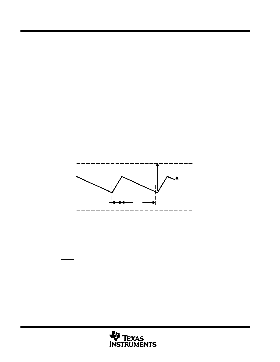
Figure 40 shows the approximate voltage waveform at AIN resulting from clamp droop during td and clamp
voltage reacquisition during the clamp pulse time, tc.
V
COS
VDROOP = VAIN
tc
td
V(Clamp)
VAIN
VM
Figure 40. Approximate Waveforms at AIN During Droop and Clamping
The voltage change at AIN during acquisition has been approximated as a linear charging ramp by assuming
that almost all of VCOS appears across RIN, giving a charging current VCOS/Rin (this is a reasonable
approximation when VCOS is large enough to be a problem). The voltage change at AIN during clamp acquisition
is then
DV
AIN +
V
COS
R
IN
tc
The peak-to-peak voltage variation at AIN must equal the clamp droop voltage at steady state. Equating the
droop voltage to the clamp acquisition voltage change gives
V
COS +
R
IN
I
IN
td
tc
Where IIN is the input current given by equation, thus for low offset voltage, keep RIN low and ensure that the
ratio td/tc is not unreasonably large.
(24)
(25)
相关PDF资料 |
PDF描述 |
|---|---|
| THS1031CDWG4 | 1-CH 10-BIT PROPRIETARY METHOD ADC, PARALLEL ACCESS, PDSO28 |
| THS1031CPWG4 | 1-CH 10-BIT PROPRIETARY METHOD ADC, PARALLEL ACCESS, PDSO28 |
| THS1031CPWR | 1-CH 10-BIT PROPRIETARY METHOD ADC, PARALLEL ACCESS, PDSO28 |
| THS1031IPWLE | 10-CH 10-BIT PROPRIETARY METHOD ADC, PARALLEL ACCESS, PDSO28 |
| THS1031CPWLE | 10-CH 10-BIT PROPRIETARY METHOD ADC, PARALLEL ACCESS, PDSO28 |
相关代理商/技术参数 |
参数描述 |
|---|---|
| THS1031IDWR | 功能描述:模数转换器 - ADC 10-Bit 30 MSPS 1-Ch RoHS:否 制造商:Texas Instruments 通道数量:2 结构:Sigma-Delta 转换速率:125 SPs to 8 KSPs 分辨率:24 bit 输入类型:Differential 信噪比:107 dB 接口类型:SPI 工作电源电压:1.7 V to 3.6 V, 2.7 V to 5.25 V 最大工作温度:+ 85 C 安装风格:SMD/SMT 封装 / 箱体:VQFN-32 |
| THS1031IDWRG4 | 功能描述:模数转换器 - ADC 10-Bit 30 MSPS 1-Ch RoHS:否 制造商:Texas Instruments 通道数量:2 结构:Sigma-Delta 转换速率:125 SPs to 8 KSPs 分辨率:24 bit 输入类型:Differential 信噪比:107 dB 接口类型:SPI 工作电源电压:1.7 V to 3.6 V, 2.7 V to 5.25 V 最大工作温度:+ 85 C 安装风格:SMD/SMT 封装 / 箱体:VQFN-32 |
| THS1031IPW | 功能描述:模数转换器 - ADC _ RoHS:否 制造商:Texas Instruments 通道数量:2 结构:Sigma-Delta 转换速率:125 SPs to 8 KSPs 分辨率:24 bit 输入类型:Differential 信噪比:107 dB 接口类型:SPI 工作电源电压:1.7 V to 3.6 V, 2.7 V to 5.25 V 最大工作温度:+ 85 C 安装风格:SMD/SMT 封装 / 箱体:VQFN-32 |
| THS1031IPWG4 | 功能描述:模数转换器 - ADC 10B 30 MSPS ADC Sgl Ch. Integ. Pgmable RoHS:否 制造商:Texas Instruments 通道数量:2 结构:Sigma-Delta 转换速率:125 SPs to 8 KSPs 分辨率:24 bit 输入类型:Differential 信噪比:107 dB 接口类型:SPI 工作电源电压:1.7 V to 3.6 V, 2.7 V to 5.25 V 最大工作温度:+ 85 C 安装风格:SMD/SMT 封装 / 箱体:VQFN-32 |
| THS1031IPWR | 功能描述:模数转换器 - ADC 10-Bit 30 MSPS 1-Ch RoHS:否 制造商:Texas Instruments 通道数量:2 结构:Sigma-Delta 转换速率:125 SPs to 8 KSPs 分辨率:24 bit 输入类型:Differential 信噪比:107 dB 接口类型:SPI 工作电源电压:1.7 V to 3.6 V, 2.7 V to 5.25 V 最大工作温度:+ 85 C 安装风格:SMD/SMT 封装 / 箱体:VQFN-32 |
发布紧急采购,3分钟左右您将得到回复。