- 您现在的位置:买卖IC网 > PDF目录98217 > THS1031IDWG4 (TEXAS INSTRUMENTS INC) 1-CH 10-BIT PROPRIETARY METHOD ADC, PARALLEL ACCESS, PDSO28 PDF资料下载
参数资料
| 型号: | THS1031IDWG4 |
| 厂商: | TEXAS INSTRUMENTS INC |
| 元件分类: | ADC |
| 英文描述: | 1-CH 10-BIT PROPRIETARY METHOD ADC, PARALLEL ACCESS, PDSO28 |
| 封装: | GREEN, PLASTIC, SOIC-28 |
| 文件页数: | 21/41页 |
| 文件大小: | 728K |
| 代理商: | THS1031IDWG4 |
第1页第2页第3页第4页第5页第6页第7页第8页第9页第10页第11页第12页第13页第14页第15页第16页第17页第18页第19页第20页当前第21页第22页第23页第24页第25页第26页第27页第28页第29页第30页第31页第32页第33页第34页第35页第36页第37页第38页第39页第40页第41页
THS1031
3-V TO 5.5-V, 10-BIT, 30 MSPS
CMOS ANALOG-TO-DIGITAL CONVERTER
SLAS242E – NOVEMBER 1999 – REVISED MARCH 2002
28
POST OFFICE BOX 655303
DALLAS, TEXAS 75265
PRINCIPLES OF OPERATION
driving the THS1301 analog inputs
driving AIN
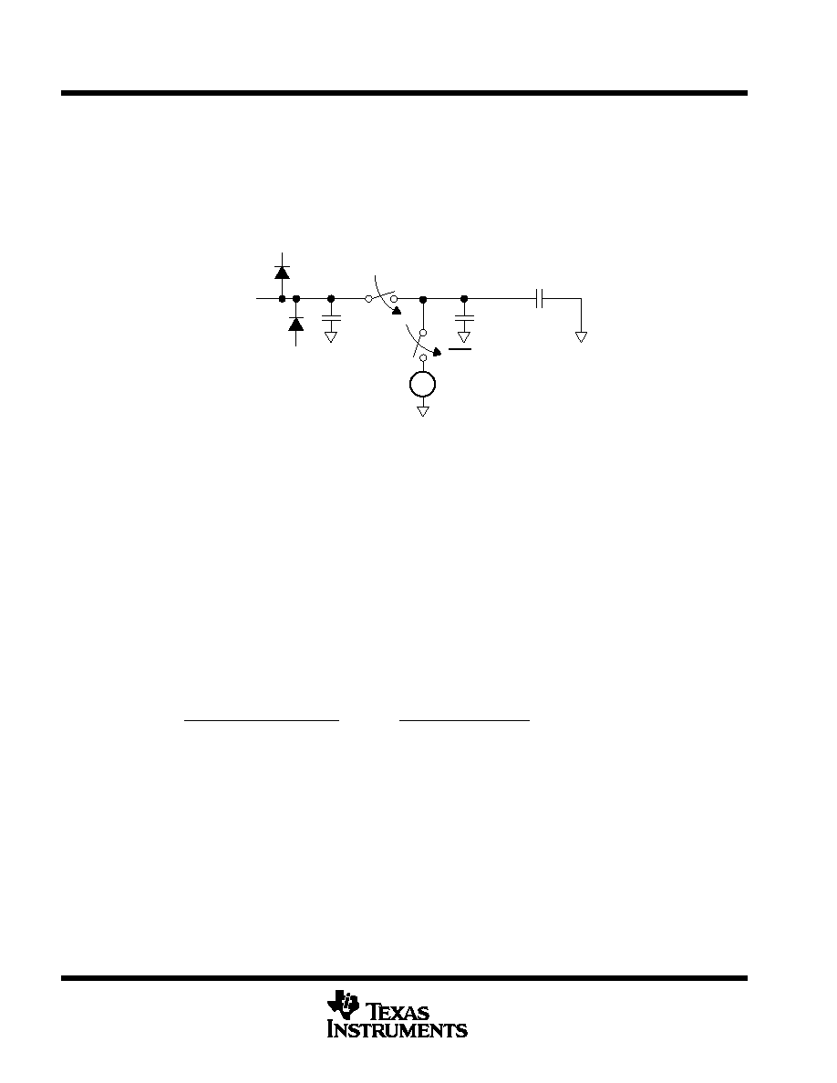
Figure 32 shows an equivalent circuit for the THS1031 AIN pin. The load presented to the system at the AIN
pin comprises the switched input sampling capacitor, CSAMPLE, and various stray capacitances, CP1 and CP2.
C1
8 pF
AVDD
AGND
CLK
C2
1.2 pF
CSAMPLE
VLAST
AIN
_
+
Figure 32. Equivalent Circuit of Analog Input AIN
In any single-ended input mode, VLAST = the average of the previously sampled voltage at AIN and the average
of the voltages on pins REFTS and REFBS. In any differential mode, VLAST = the common mode input voltage.
The external source driving AIN must be able to charge and settle into CSAMPLE and the CP1 and CP2 strays
to within 0.5 LSB error while sampling (CLK pin low) to achieve full ADC resolution.
AIN input current and input load modeling
When CLK goes low, the source driving AIN must charge the total switched capacitance CS = CSAMPLE + CP2.
The total charge transferred depends on the voltage at AIN and is given by
Q
CHARGING +
(AIN
* V
LAST
)
C
S
.
For a fixed voltage at AIN, so that AIN and VLAST do not change between samples, the maximum amount of
charge transfer occurs at AIN = FS– (charging current flows out of THS1030) and AIN = FS+ (current flows into
THS1030). If AIN is held at the voltage FS+, VLAST = [(FS+) + VM]/2, giving a maximum transferred charge:
Q(FS)
+
(FS
)) * [(FS )) ) VM]
2
C
S +
[(FS
)) * VM]
C
S
2
+ (1 4 of the input voltage span)
C
S
If the input voltage changes between samples, then the maximum possible charge transfer is
Q(max)
+ 3
Q(FS)
which occurs for a full-scale input change (FS+ to FS– or FS– to FS+) between samples.
The charging current pulses can make the AIN source jump or ring, especially if the source is slightly inductive
at high frequencies. Inserting a small series resistor of 20
or less in the input path can damp source ringing.
See Figure 33. This resistor can be made larger than 20
if reduced input bandwidth or distortion performance
is acceptable.
(9)
(10)
(11)
相关PDF资料 |
PDF描述 |
|---|---|
| THS1031CDWG4 | 1-CH 10-BIT PROPRIETARY METHOD ADC, PARALLEL ACCESS, PDSO28 |
| THS1031CPWG4 | 1-CH 10-BIT PROPRIETARY METHOD ADC, PARALLEL ACCESS, PDSO28 |
| THS1031CPWR | 1-CH 10-BIT PROPRIETARY METHOD ADC, PARALLEL ACCESS, PDSO28 |
| THS1031IPWLE | 10-CH 10-BIT PROPRIETARY METHOD ADC, PARALLEL ACCESS, PDSO28 |
| THS1031CPWLE | 10-CH 10-BIT PROPRIETARY METHOD ADC, PARALLEL ACCESS, PDSO28 |
相关代理商/技术参数 |
参数描述 |
|---|---|
| THS1031IDWR | 功能描述:模数转换器 - ADC 10-Bit 30 MSPS 1-Ch RoHS:否 制造商:Texas Instruments 通道数量:2 结构:Sigma-Delta 转换速率:125 SPs to 8 KSPs 分辨率:24 bit 输入类型:Differential 信噪比:107 dB 接口类型:SPI 工作电源电压:1.7 V to 3.6 V, 2.7 V to 5.25 V 最大工作温度:+ 85 C 安装风格:SMD/SMT 封装 / 箱体:VQFN-32 |
| THS1031IDWRG4 | 功能描述:模数转换器 - ADC 10-Bit 30 MSPS 1-Ch RoHS:否 制造商:Texas Instruments 通道数量:2 结构:Sigma-Delta 转换速率:125 SPs to 8 KSPs 分辨率:24 bit 输入类型:Differential 信噪比:107 dB 接口类型:SPI 工作电源电压:1.7 V to 3.6 V, 2.7 V to 5.25 V 最大工作温度:+ 85 C 安装风格:SMD/SMT 封装 / 箱体:VQFN-32 |
| THS1031IPW | 功能描述:模数转换器 - ADC _ RoHS:否 制造商:Texas Instruments 通道数量:2 结构:Sigma-Delta 转换速率:125 SPs to 8 KSPs 分辨率:24 bit 输入类型:Differential 信噪比:107 dB 接口类型:SPI 工作电源电压:1.7 V to 3.6 V, 2.7 V to 5.25 V 最大工作温度:+ 85 C 安装风格:SMD/SMT 封装 / 箱体:VQFN-32 |
| THS1031IPWG4 | 功能描述:模数转换器 - ADC 10B 30 MSPS ADC Sgl Ch. Integ. Pgmable RoHS:否 制造商:Texas Instruments 通道数量:2 结构:Sigma-Delta 转换速率:125 SPs to 8 KSPs 分辨率:24 bit 输入类型:Differential 信噪比:107 dB 接口类型:SPI 工作电源电压:1.7 V to 3.6 V, 2.7 V to 5.25 V 最大工作温度:+ 85 C 安装风格:SMD/SMT 封装 / 箱体:VQFN-32 |
| THS1031IPWR | 功能描述:模数转换器 - ADC 10-Bit 30 MSPS 1-Ch RoHS:否 制造商:Texas Instruments 通道数量:2 结构:Sigma-Delta 转换速率:125 SPs to 8 KSPs 分辨率:24 bit 输入类型:Differential 信噪比:107 dB 接口类型:SPI 工作电源电压:1.7 V to 3.6 V, 2.7 V to 5.25 V 最大工作温度:+ 85 C 安装风格:SMD/SMT 封装 / 箱体:VQFN-32 |
发布紧急采购,3分钟左右您将得到回复。