- 您现在的位置:买卖IC网 > PDF目录98219 > THS1215CPWRG4 (TEXAS INSTRUMENTS INC) 1-CH 12-BIT PROPRIETARY METHOD ADC, PARALLEL ACCESS, PDSO28 PDF资料下载
参数资料
| 型号: | THS1215CPWRG4 |
| 厂商: | TEXAS INSTRUMENTS INC |
| 元件分类: | ADC |
| 英文描述: | 1-CH 12-BIT PROPRIETARY METHOD ADC, PARALLEL ACCESS, PDSO28 |
| 封装: | GREEN, PLASTIC, TSSOP-28 |
| 文件页数: | 18/24页 |
| 文件大小: | 539K |
| 代理商: | THS1215CPWRG4 |
www.ti.com
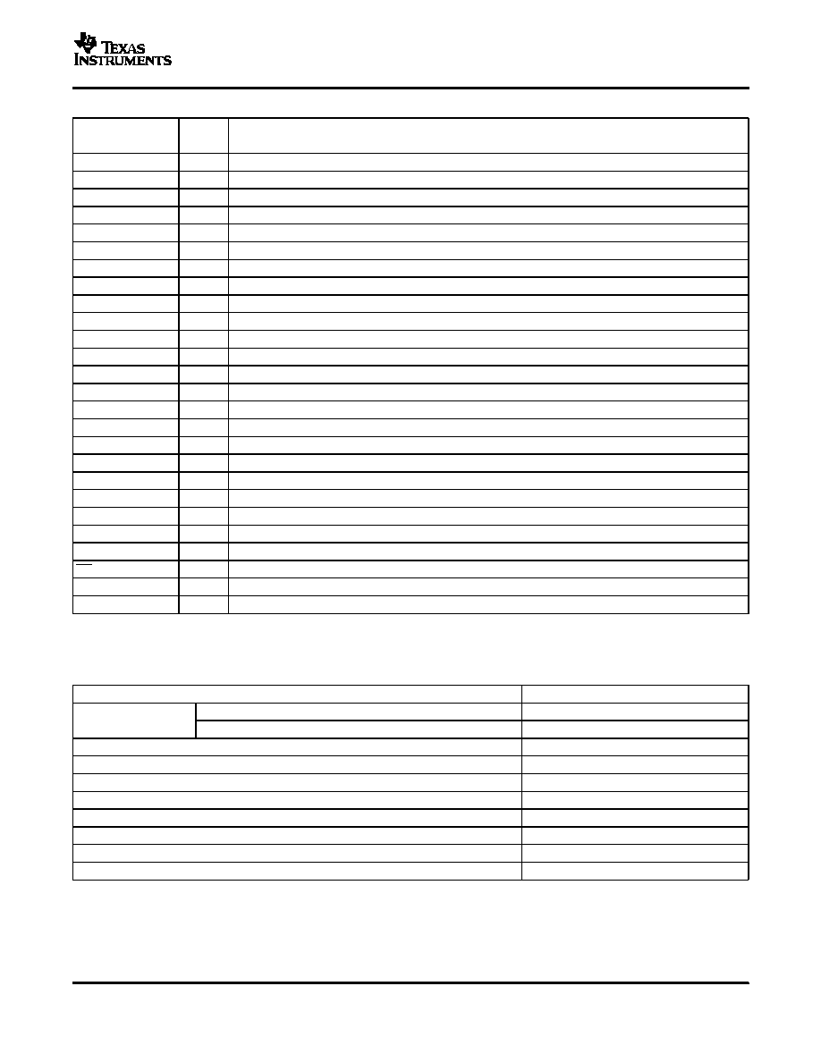
TERMINAL FUNCTIONS
ABSOLUTE MAXIMUM RATINGS
(1)
THS1215
SLAS292A – MARCH 2001 – REVISED MARCH 2004
TERMINAL
I/O
DESCRIPTION
NAME
NO.
AGND
1, 7
I
Analog ground
AVDD
8, 27
I
Analog supply
AIN+
5
I
Positive analog input
AIN-
6
I
Negative analog input
CLK
28
I
ADC conversion clock
CON1
2
I
Configuration input 1
CON0
3
I
Configuration input 0
DGND
19
I
Digital ground
DVDD
20
I
Digital supply
D11
12
O
ADC data bit 11
D10
13
O
ADC data bit 10
D9
14
O
ADC data bit 9
D8
15
O
ADC data bit 8
D7
16
O
ADC data bit 7
D6
17
O
ADC data bit 6
D5
18
O
ADC data bit 5
D4
21
O
ADC data bit 4
D3
22
O
ADC data bit 3
D2
23
O
ADC data bit 2
D1
24
O
ADC data bit 1
D0
25
O
ADC data bit 0
EXTREF
4
I
Reference select input (high = external, low = internal)
OVRNG
11
O
Out of range indicator (high = out of range)
OE
26
I
Output enable (high = disable, low = enable)
REFT
9
I/O
Upper ADC reference voltage
REFB
10
I/O
Lower ADC reference voltage
over operating free-air temperature range (unless otherwise noted)
UNIT
AVDD to AGND, DVDD to DGND
–0.3 V to 4 V
Supply voltage range
AGND to DGND
–0.3 V to 0.3 V
Reference voltage input range, REFT, REFB to AGND
–0.3 to AVDD + 0.3 V
Analog input voltage range, AIN+, AIN– to AGND
–0.3 to AVDD + 0.3 V
Clock input voltage range, CLK to AGND
–0.3 to AVDD + 0.3 V
Digital input voltage range, digital input to DGND
–0.3 to DVDD + 0.3 V
Digital output voltage range, digital output to DGND
–0.3 to DVDD + 0.3 V
Operating junction temperature range, TJ
–40
°C to 150°C
Storage temperature range, TSTG
–65
°C to 150°C
Lead temperature 1,6 mm (1/16 in) from case for 10 seconds
300
°C
(1)
Stresses beyond those listed under "absolute maximum ratings" may cause permanent damage to the device. These are stress ratings
only, and functional operation of the device at these or any other conditions beyond those indicated under "recommended operating
conditions" is not implied. Exposure to absolute-maximum-rated conditions for extended periods may affect device reliability.
3
相关PDF资料 |
PDF描述 |
|---|---|
| THS1215CDW | 1-CH 12-BIT PROPRIETARY METHOD ADC, PARALLEL ACCESS, PDSO28 |
| THS1215CPW | 1-CH 12-BIT PROPRIETARY METHOD ADC, PARALLEL ACCESS, PDSO28 |
| THS1215IDW | 1-CH 12-BIT PROPRIETARY METHOD ADC, PARALLEL ACCESS, PDSO28 |
| THS1215CDWR | 1-CH 12-BIT PROPRIETARY METHOD ADC, PARALLEL ACCESS, PDSO28 |
| THS1215IPWR | 1-CH 12-BIT PROPRIETARY METHOD ADC, PARALLEL ACCESS, PDSO28 |
相关代理商/技术参数 |
参数描述 |
|---|---|
| THS1215EVM | 功能描述:数据转换 IC 开发工具 THS1215 Eval Mod RoHS:否 制造商:Texas Instruments 产品:Demonstration Kits 类型:ADC 工具用于评估:ADS130E08 接口类型:SPI 工作电源电压:- 6 V to + 6 V |
| THS1215IDW | 功能描述:模数转换器 - ADC 12-Bit 15 MSPS w/Low Pwr & exc ENOB RoHS:否 制造商:Texas Instruments 通道数量:2 结构:Sigma-Delta 转换速率:125 SPs to 8 KSPs 分辨率:24 bit 输入类型:Differential 信噪比:107 dB 接口类型:SPI 工作电源电压:1.7 V to 3.6 V, 2.7 V to 5.25 V 最大工作温度:+ 85 C 安装风格:SMD/SMT 封装 / 箱体:VQFN-32 |
| THS1215IDWG4 | 功能描述:模数转换器 - ADC 12-Bit 15 MSPS w/Low Pwr & exc ENOB RoHS:否 制造商:Texas Instruments 通道数量:2 结构:Sigma-Delta 转换速率:125 SPs to 8 KSPs 分辨率:24 bit 输入类型:Differential 信噪比:107 dB 接口类型:SPI 工作电源电压:1.7 V to 3.6 V, 2.7 V to 5.25 V 最大工作温度:+ 85 C 安装风格:SMD/SMT 封装 / 箱体:VQFN-32 |
| THS1215IDWR | 功能描述:模数转换器 - ADC 12-Bit 15 MSPS w/Low Pwr & exc ENOB RoHS:否 制造商:Texas Instruments 通道数量:2 结构:Sigma-Delta 转换速率:125 SPs to 8 KSPs 分辨率:24 bit 输入类型:Differential 信噪比:107 dB 接口类型:SPI 工作电源电压:1.7 V to 3.6 V, 2.7 V to 5.25 V 最大工作温度:+ 85 C 安装风格:SMD/SMT 封装 / 箱体:VQFN-32 |
| THS1215IDWRG4 | 功能描述:模数转换器 - ADC 12-Bit 15 MSPS w/Low Pwr & exc ENOB RoHS:否 制造商:Texas Instruments 通道数量:2 结构:Sigma-Delta 转换速率:125 SPs to 8 KSPs 分辨率:24 bit 输入类型:Differential 信噪比:107 dB 接口类型:SPI 工作电源电压:1.7 V to 3.6 V, 2.7 V to 5.25 V 最大工作温度:+ 85 C 安装风格:SMD/SMT 封装 / 箱体:VQFN-32 |
发布紧急采购,3分钟左右您将得到回复。