- 您现在的位置:买卖IC网 > PDF目录98219 > THS1215CPWRG4 (TEXAS INSTRUMENTS INC) 1-CH 12-BIT PROPRIETARY METHOD ADC, PARALLEL ACCESS, PDSO28 PDF资料下载
参数资料
| 型号: | THS1215CPWRG4 |
| 厂商: | TEXAS INSTRUMENTS INC |
| 元件分类: | ADC |
| 英文描述: | 1-CH 12-BIT PROPRIETARY METHOD ADC, PARALLEL ACCESS, PDSO28 |
| 封装: | GREEN, PLASTIC, TSSOP-28 |
| 文件页数: | 4/24页 |
| 文件大小: | 539K |
| 代理商: | THS1215CPWRG4 |
www.ti.com
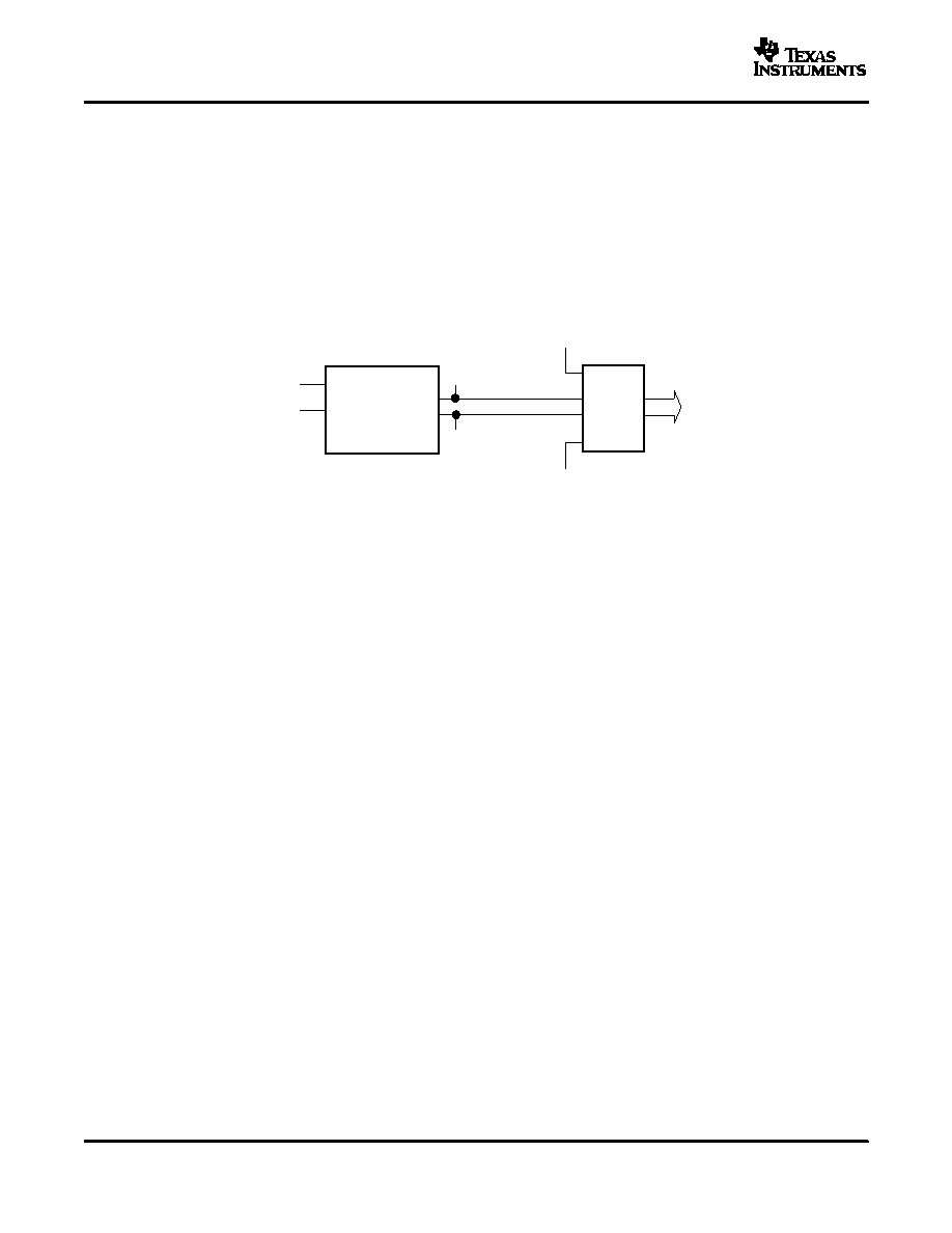
SIGNAL PROCESSING CHAIN (Sample and Hold, ADC)
SAMPLE
AND
HOLD
AIN
AIN+
+1
1
VP+
VP
REFT
REFB
ADC
CORE
Sample and Hold
Analog-to-Digital Converter
Analog input
THS1215
SLAS292A – MARCH 2001 – REVISED MARCH 2004
Table 2 assumes that the delta in ADC reference voltages VREFT and VREFB is set to 1 V, i.e., VREFT – VREFB = 1
V. Note that VREFB and VREFT can be set externally, which will scale the numbers given in this table.
The user-chosen operating configuration and reference voltages determine what input signal voltage range the
THS1215 can handle.
The following sections explain both the internal signal flow of the device and how the input signal span is related
to the ADC reference voltages, as well as the ways in which the ADC reference voltages can be buffered
internally or externally applied.
Figure 15 shows the signal flow through the sample and hold unit and the PGA to the ADC core.
Figure 15. Analog Input Signal Flow
The differential sample and hold processes AIN with respect to the voltages applied to the REFT and REFB pins,
to give a differential output (VP+) – (VP–) = VP given by:
VP = (AIN+) – ( AIN–)
No matter what operating configuration is chosen, VP is digitized against ADC reference voltages VREFT and
VREFB. The VREFT and VREFB voltages set the analog input span limits FS+ and FS–, respectively. Any voltages at
AIN greater than REFT or less than REFB causes ADC over-range, which is signaled by OVR going high when
the conversion result is output.
A first-order approximation for the equivalent analog input circuit of the THS1215 is shown in Figure 16. The
equivalent input capacitance CI is 5 pF typical. The input must charge/discharge this capacitance within the
sample period of one half of a clock cycle. When a full-scale voltage step is applied, the input source provides
the charging current through the switch resistance RSW (200 ) of S1 and quickly settles. In this case the input
impedance is low. Alternatively, when the source voltage equals the value previously stored on CI, the hold
capacitor requires no input current and the equivalent input impedance is high.
12
相关PDF资料 |
PDF描述 |
|---|---|
| THS1215CDW | 1-CH 12-BIT PROPRIETARY METHOD ADC, PARALLEL ACCESS, PDSO28 |
| THS1215CPW | 1-CH 12-BIT PROPRIETARY METHOD ADC, PARALLEL ACCESS, PDSO28 |
| THS1215IDW | 1-CH 12-BIT PROPRIETARY METHOD ADC, PARALLEL ACCESS, PDSO28 |
| THS1215CDWR | 1-CH 12-BIT PROPRIETARY METHOD ADC, PARALLEL ACCESS, PDSO28 |
| THS1215IPWR | 1-CH 12-BIT PROPRIETARY METHOD ADC, PARALLEL ACCESS, PDSO28 |
相关代理商/技术参数 |
参数描述 |
|---|---|
| THS1215EVM | 功能描述:数据转换 IC 开发工具 THS1215 Eval Mod RoHS:否 制造商:Texas Instruments 产品:Demonstration Kits 类型:ADC 工具用于评估:ADS130E08 接口类型:SPI 工作电源电压:- 6 V to + 6 V |
| THS1215IDW | 功能描述:模数转换器 - ADC 12-Bit 15 MSPS w/Low Pwr & exc ENOB RoHS:否 制造商:Texas Instruments 通道数量:2 结构:Sigma-Delta 转换速率:125 SPs to 8 KSPs 分辨率:24 bit 输入类型:Differential 信噪比:107 dB 接口类型:SPI 工作电源电压:1.7 V to 3.6 V, 2.7 V to 5.25 V 最大工作温度:+ 85 C 安装风格:SMD/SMT 封装 / 箱体:VQFN-32 |
| THS1215IDWG4 | 功能描述:模数转换器 - ADC 12-Bit 15 MSPS w/Low Pwr & exc ENOB RoHS:否 制造商:Texas Instruments 通道数量:2 结构:Sigma-Delta 转换速率:125 SPs to 8 KSPs 分辨率:24 bit 输入类型:Differential 信噪比:107 dB 接口类型:SPI 工作电源电压:1.7 V to 3.6 V, 2.7 V to 5.25 V 最大工作温度:+ 85 C 安装风格:SMD/SMT 封装 / 箱体:VQFN-32 |
| THS1215IDWR | 功能描述:模数转换器 - ADC 12-Bit 15 MSPS w/Low Pwr & exc ENOB RoHS:否 制造商:Texas Instruments 通道数量:2 结构:Sigma-Delta 转换速率:125 SPs to 8 KSPs 分辨率:24 bit 输入类型:Differential 信噪比:107 dB 接口类型:SPI 工作电源电压:1.7 V to 3.6 V, 2.7 V to 5.25 V 最大工作温度:+ 85 C 安装风格:SMD/SMT 封装 / 箱体:VQFN-32 |
| THS1215IDWRG4 | 功能描述:模数转换器 - ADC 12-Bit 15 MSPS w/Low Pwr & exc ENOB RoHS:否 制造商:Texas Instruments 通道数量:2 结构:Sigma-Delta 转换速率:125 SPs to 8 KSPs 分辨率:24 bit 输入类型:Differential 信噪比:107 dB 接口类型:SPI 工作电源电压:1.7 V to 3.6 V, 2.7 V to 5.25 V 最大工作温度:+ 85 C 安装风格:SMD/SMT 封装 / 箱体:VQFN-32 |
发布紧急采购,3分钟左右您将得到回复。