- 您现在的位置:买卖IC网 > PDF目录98219 > THS1215CPWRG4 (TEXAS INSTRUMENTS INC) 1-CH 12-BIT PROPRIETARY METHOD ADC, PARALLEL ACCESS, PDSO28 PDF资料下载
参数资料
| 型号: | THS1215CPWRG4 |
| 厂商: | TEXAS INSTRUMENTS INC |
| 元件分类: | ADC |
| 英文描述: | 1-CH 12-BIT PROPRIETARY METHOD ADC, PARALLEL ACCESS, PDSO28 |
| 封装: | GREEN, PLASTIC, TSSOP-28 |
| 文件页数: | 3/24页 |
| 文件大小: | 539K |
| 代理商: | THS1215CPWRG4 |
www.ti.com
PRINCIPLES OF OPERATION
ANALOG INPUT
AIN
0
4095
2V
MODE 2, CON[1:0] = 10
OUTPUT
CODE
AIN
0
4095
1V
MODE 1, CON[1:0] = 01
OUTPUT
CODE
AIN+
THS1215
SLAS292A – MARCH 2001 – REVISED MARCH 2004
The analog input AIN is sampled in the sample and hold unit, the output of which feeds the ADC CORE, where
the process of analog-to-digital conversion is performed against ADC reference voltages, VREFT and VREFB.
Connecting the EXTREF pin to one of two voltages, DGND or DVDD selects one of the two configurations of ADC
reference generation. The ADC reference voltages come from either the internal reference buffer or completely
external sources. Connect EXTREF to DGND for internal reference generation or to DVDD for external reference
generation.
CON0 and CON1 as described below, select the input configuration mode or place the device in power-down
state. The ADC core drives out through output buffers to the data pins D0 to D11. The output buffers can be
disabled by the OE pin.
A single, sample-rate clock (15 MHz maximum) is required at pin CLK. The analog input signal is sampled on the
rising edge of CLK, and corresponding data is output after the fifth following rising edge.
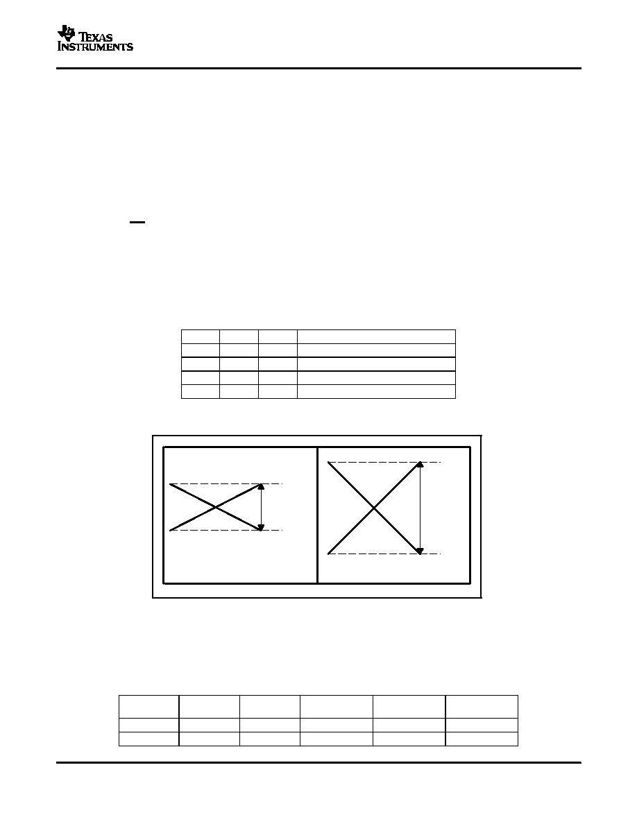
The THS1215 can operate in differential Mode 1 or differential Mode 2, controlled by the configuration pins
CON0 and CON1 as shown in Table 1. Mode 0 places the THS1215 in power-down or standby state for reduced
power consumption.
Table 1. Input Modes of Operation
MODE
CON1
CON0
MODE OF OPERATION
0
Device powered down
1
0
1
Differential mode
× 1
2
1
0
Differential mode
× 0.5
3
1
Not used
Modes 1 and 2 are shown in Figure 14.
Figure 14. Input Mode Configurations
The gain of the sample and hold changes with the CON1 and the CON0 inputs. Table 2 shows the gain of the
sample and hold and the levels applied at the AIN+ and AIN– analog inputs for Mode 1 and Mode 2. The
common mode level for the two analog inputs is at AVDD/2.
Table 2. Input Mode Switching
(AIN+) – (AIN-)
MODE
CON1
CON0
S/H GAIN
MIN
MAX
1
0
1
–1 V
1 V
×1
2
1
0
-2 V
2 V
×0.5
11
相关PDF资料 |
PDF描述 |
|---|---|
| THS1215CDW | 1-CH 12-BIT PROPRIETARY METHOD ADC, PARALLEL ACCESS, PDSO28 |
| THS1215CPW | 1-CH 12-BIT PROPRIETARY METHOD ADC, PARALLEL ACCESS, PDSO28 |
| THS1215IDW | 1-CH 12-BIT PROPRIETARY METHOD ADC, PARALLEL ACCESS, PDSO28 |
| THS1215CDWR | 1-CH 12-BIT PROPRIETARY METHOD ADC, PARALLEL ACCESS, PDSO28 |
| THS1215IPWR | 1-CH 12-BIT PROPRIETARY METHOD ADC, PARALLEL ACCESS, PDSO28 |
相关代理商/技术参数 |
参数描述 |
|---|---|
| THS1215EVM | 功能描述:数据转换 IC 开发工具 THS1215 Eval Mod RoHS:否 制造商:Texas Instruments 产品:Demonstration Kits 类型:ADC 工具用于评估:ADS130E08 接口类型:SPI 工作电源电压:- 6 V to + 6 V |
| THS1215IDW | 功能描述:模数转换器 - ADC 12-Bit 15 MSPS w/Low Pwr & exc ENOB RoHS:否 制造商:Texas Instruments 通道数量:2 结构:Sigma-Delta 转换速率:125 SPs to 8 KSPs 分辨率:24 bit 输入类型:Differential 信噪比:107 dB 接口类型:SPI 工作电源电压:1.7 V to 3.6 V, 2.7 V to 5.25 V 最大工作温度:+ 85 C 安装风格:SMD/SMT 封装 / 箱体:VQFN-32 |
| THS1215IDWG4 | 功能描述:模数转换器 - ADC 12-Bit 15 MSPS w/Low Pwr & exc ENOB RoHS:否 制造商:Texas Instruments 通道数量:2 结构:Sigma-Delta 转换速率:125 SPs to 8 KSPs 分辨率:24 bit 输入类型:Differential 信噪比:107 dB 接口类型:SPI 工作电源电压:1.7 V to 3.6 V, 2.7 V to 5.25 V 最大工作温度:+ 85 C 安装风格:SMD/SMT 封装 / 箱体:VQFN-32 |
| THS1215IDWR | 功能描述:模数转换器 - ADC 12-Bit 15 MSPS w/Low Pwr & exc ENOB RoHS:否 制造商:Texas Instruments 通道数量:2 结构:Sigma-Delta 转换速率:125 SPs to 8 KSPs 分辨率:24 bit 输入类型:Differential 信噪比:107 dB 接口类型:SPI 工作电源电压:1.7 V to 3.6 V, 2.7 V to 5.25 V 最大工作温度:+ 85 C 安装风格:SMD/SMT 封装 / 箱体:VQFN-32 |
| THS1215IDWRG4 | 功能描述:模数转换器 - ADC 12-Bit 15 MSPS w/Low Pwr & exc ENOB RoHS:否 制造商:Texas Instruments 通道数量:2 结构:Sigma-Delta 转换速率:125 SPs to 8 KSPs 分辨率:24 bit 输入类型:Differential 信噪比:107 dB 接口类型:SPI 工作电源电压:1.7 V to 3.6 V, 2.7 V to 5.25 V 最大工作温度:+ 85 C 安装风格:SMD/SMT 封装 / 箱体:VQFN-32 |
发布紧急采购,3分钟左右您将得到回复。