- 您现在的位置:买卖IC网 > PDF目录98224 > THS4211DRB (TEXAS INSTRUMENTS INC) 1 CHANNEL, VIDEO AMPLIFIER, PDSO8 PDF资料下载
参数资料
| 型号: | THS4211DRB |
| 厂商: | TEXAS INSTRUMENTS INC |
| 元件分类: | 音频/视频放大 |
| 英文描述: | 1 CHANNEL, VIDEO AMPLIFIER, PDSO8 |
| 封装: | PLASTIC, MSOP-8 |
| 文件页数: | 17/40页 |
| 文件大小: | 1013K |
| 代理商: | THS4211DRB |
第1页第2页第3页第4页第5页第6页第7页第8页第9页第10页第11页第12页第13页第14页第15页第16页当前第17页第18页第19页第20页第21页第22页第23页第24页第25页第26页第27页第28页第29页第30页第31页第32页第33页第34页第35页第36页第37页第38页第39页第40页
THS4211
THS4215
SLOS400C SEPTEMBER 2002 REVISED JANUARY 2004
www.ti.com
24
_
+
Rf
4kT = 1.6E20J
at 290K
THS4211/THS4215
IBN
EO
ERF
RS
ERS
IBI
Rg
ENI
4kTRS
4kT
Rg
4kTRf
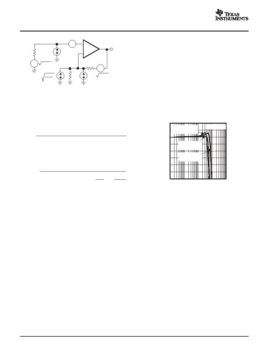
Figure 87. Noise Analysis Model
The total output shot noise voltage can be computed as the
square of all square output noise voltage contributors.
Equation 3 shows the general form for the output noise
voltage using the terms shown in Figure 87:
E
O +
E 2
NI
) I
BNRS
2
) 4kTR
S NG
2
) I
BIRf
2
) 4kTR
fNG
Dividing this expression by the noise gain (NG=(1+ Rf/Rg))
gives the equivalent input-referred spot noise voltage at
the noninverting input, as shown in Equation 4:
E
O +
E 2
NI
) I
BNRS
2 ) 4kTR
S )
I
BIRf
NG
2
)
4kTR
f
NG
Driving Capacitive Loads
One of the most demanding, and yet very common, load
conditions for an op amp is capacitive loading. Often, the
capacitive load is the input of an A/D converter, including
additional
external
capacitance,
which
may
be
recommended to improve A/D linearity. A high-speed, high
open-loop gain amplifier like the THS4211 can be very
susceptible to decreased stability and closed-loop
response peaking when a capacitive load is placed directly
on the output pin. When the amplifier’s open-loop output
resistance is considered, this capacitive load introduces
an additional pole in the signal path that can decrease the
phase margin. When the primary considerations are
frequency response flatness, pulse response fidelity, or
distortion, the simplest and most effective solution is to
isolate the capacitive load from the feedback loop by
inserting a series isolation resistor between the amplifier
output and the capacitive load. This does not eliminate the
pole from the loop response, but rather shifts it and adds
a zero at a higher frequency. The additional zero acts to
cancel the phase lag from the capacitive load pole, thus
increasing the phase margin and improving stability.
The Typical Characteristics show the recommended
isolation resistor vs capacitive load and the resulting
frequency response at the load. Parasitic capacitive loads
greater than 2 pF can begin to degrade the performance
of the THS4211. Long PC board traces, unmatched
cables, and connections to multiple devices can easily
cause this value to be exceeded. Always consider this
effect carefully, and add the recommended series resistor
as close as possible to the THS4211 output pin (see Board
Layout Guidelines).
The criterion for setting this R(ISO) resistor is a maximum
bandwidth, flat frequency response at the load. For a gain
of +2, the frequency response at the output pin is already
slightly peaked without the capacitive load, requiring
relatively high values of R(ISO) to flatten the response at
the load. Increasing the noise gain also reduces the
peaking.
3
2.5
2
1.5
1
0.5
0
0.5
1
100 k
1 M
10 M
100 M
1 G
Capacitive Load Hz
Normalized
Gain
dB
FREQUENCY RESPONSE
vs
CAPACITIVE LOAD
R(ISO) = 15
CL = 50 pF
VS =±5 V
R(ISO) = 10
CL = 100 pF
R(ISO) = 25
CL = 10 pF
Figure 88. Isolation Resistor Diagram
BOARD LAYOUT
Achieving optimum performance with a high frequency
amplifier like the THS4211 requires careful attention to
board layout parasitics and external component types.
Recommendations that optimize performance include the
following:
1.
Minimize parasitic capacitance to any ac ground
for all of the signal I/O pins. Parasitic capacitance on
the output and inverting input pins can cause
instability: on the noninverting input, it can react with
the source impedance to cause unintentional band
limiting. To reduce unwanted capacitance, a window
around the signal I/O pins should be opened in all of
the ground and power planes around those pins.
Otherwise, ground and power planes should be
unbroken elsewhere on the board.
2.
Minimize the distance (< 0.25”) from the power
supply pins to high frequency 0.1-
F de-coupling
capacitors. At the device pins, the ground and power
plane layout should not be in close proximity to the
signal I/O pins. Avoid narrow power and ground traces
to minimize inductance between the pins and the
(4)
(5)
相关PDF资料 |
PDF描述 |
|---|---|
| THS4215DRB | 1 CHANNEL, VIDEO AMPLIFIER, PDSO8 |
| THS4215DG4 | 1 CHANNEL, VIDEO AMPLIFIER, PDSO8 |
| THS4215DGNR | 1 CHANNEL, VIDEO AMPLIFIER, PDSO8 |
| THS4215DGN | 1 CHANNEL, VIDEO AMPLIFIER, PDSO8 |
| THS4215DRBR | 1 CHANNEL, VIDEO AMPLIFIER, PDSO8 |
相关代理商/技术参数 |
参数描述 |
|---|---|
| THS4211DRBR | 功能描述:高速运算放大器 Super-Fast Ultr-Lo- Distortion Hi-Speed RoHS:否 制造商:Texas Instruments 通道数量:1 电压增益 dB:116 dB 输入补偿电压:0.5 mV 转换速度:55 V/us 工作电源电压:36 V 电源电流:7.5 mA 最大工作温度:+ 85 C 安装风格:SMD/SMT 封装 / 箱体:SOIC-8 封装:Tube |
| THS4211DRBRG4 | 功能描述:高速运算放大器 Super-Fast Ultr-Lo- Distortion Hi-Speed RoHS:否 制造商:Texas Instruments 通道数量:1 电压增益 dB:116 dB 输入补偿电压:0.5 mV 转换速度:55 V/us 工作电源电压:36 V 电源电流:7.5 mA 最大工作温度:+ 85 C 安装风格:SMD/SMT 封装 / 箱体:SOIC-8 封装:Tube |
| THS4211DRBT | 功能描述:高速运算放大器 Super-Fast Ultr-Lo- Distortion Hi-Speed RoHS:否 制造商:Texas Instruments 通道数量:1 电压增益 dB:116 dB 输入补偿电压:0.5 mV 转换速度:55 V/us 工作电源电压:36 V 电源电流:7.5 mA 最大工作温度:+ 85 C 安装风格:SMD/SMT 封装 / 箱体:SOIC-8 封装:Tube |
| THS4211DRBTG4 | 功能描述:高速运算放大器 Super-Fast Ultr-Lo- Distortion Hi-Speed RoHS:否 制造商:Texas Instruments 通道数量:1 电压增益 dB:116 dB 输入补偿电压:0.5 mV 转换速度:55 V/us 工作电源电压:36 V 电源电流:7.5 mA 最大工作温度:+ 85 C 安装风格:SMD/SMT 封装 / 箱体:SOIC-8 封装:Tube |
| THS4211DRG4 | 功能描述:高速运算放大器 Super-Fast Ultr-Lo- Distortion Hi-Speed RoHS:否 制造商:Texas Instruments 通道数量:1 电压增益 dB:116 dB 输入补偿电压:0.5 mV 转换速度:55 V/us 工作电源电压:36 V 电源电流:7.5 mA 最大工作温度:+ 85 C 安装风格:SMD/SMT 封装 / 箱体:SOIC-8 封装:Tube |
发布紧急采购,3分钟左右您将得到回复。