- 您现在的位置:买卖IC网 > PDF目录98227 > THS4275MDGNREPR (TEXAS INSTRUMENTS INC) 1 CHANNEL, VIDEO AMPLIFIER, PDSO8 PDF资料下载
参数资料
| 型号: | THS4275MDGNREPR |
| 厂商: | TEXAS INSTRUMENTS INC |
| 元件分类: | 音频/视频放大 |
| 英文描述: | 1 CHANNEL, VIDEO AMPLIFIER, PDSO8 |
| 封装: | POWERPAD, PLASTIC, MSOP-8 |
| 文件页数: | 13/36页 |
| 文件大小: | 598K |
| 代理商: | THS4275MDGNREPR |
第1页第2页第3页第4页第5页第6页第7页第8页第9页第10页第11页第12页当前第13页第14页第15页第16页第17页第18页第19页第20页第21页第22页第23页第24页第25页第26页第27页第28页第29页第30页第31页第32页第33页第34页第35页第36页
THS4271EP
THS4275EP
SGLS270A DECEMBER 2004 REVISED APRIL 2005
www.ti.com
20
_
+
THS4271
Rg
249
RT
130
100 pF
0.1
F
6.8
F
VS
5 V
50
Source
+
VI
100 pF
0.1
F
6.8
F
+
+VS
5 V
VO
CT
0.1
F
Rf
249
RM
61.9
499
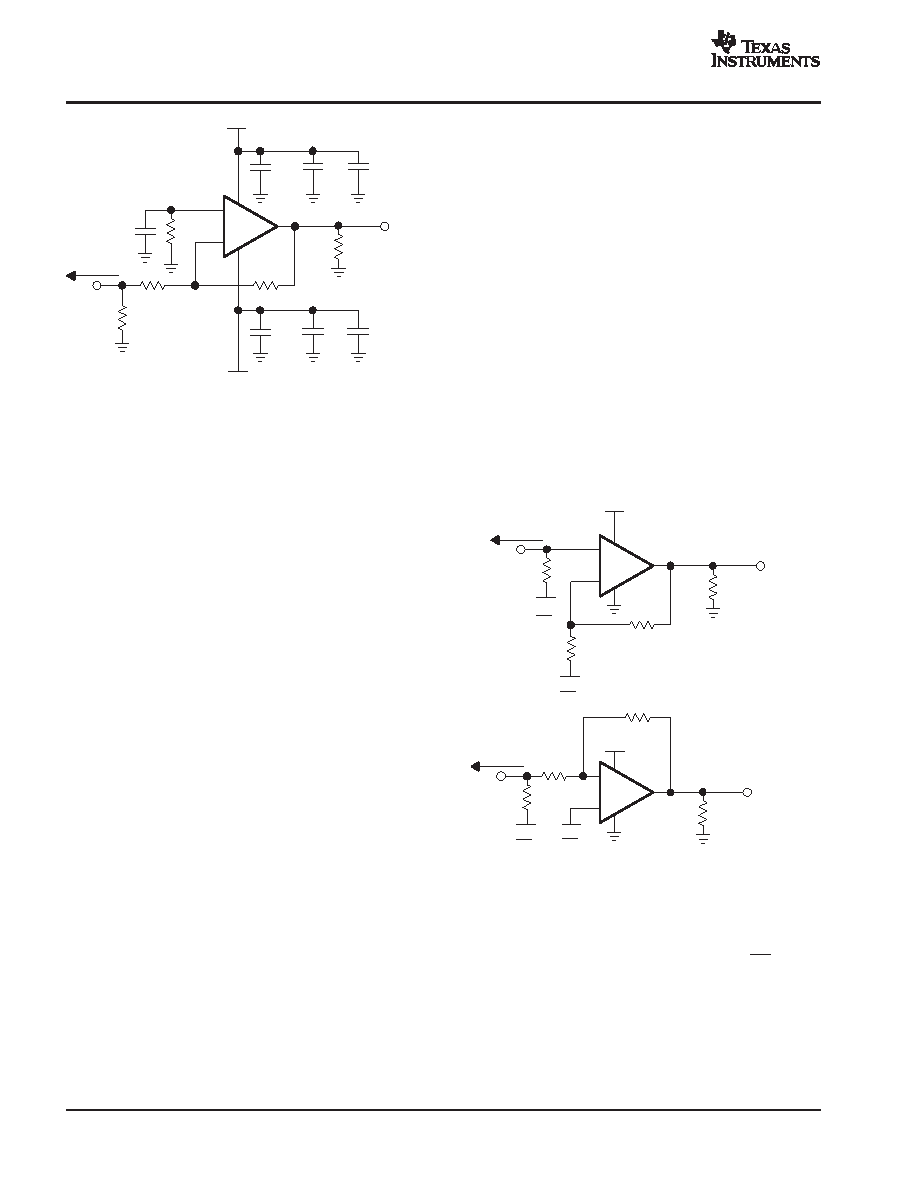
Figure 77. Wideband, Inverting Gain
Configuration
In
the
inverting
configuration,
some
key
design
considerations must be noted. One is that the gain resistor
(Rg) becomes part of the signal channel input impedance.
If the input impedance matching is desired (which is
beneficial whenever the signal is coupled through a cable,
twisted pair, long PC board trace, or other transmission
line conductors), Rg may be set equal to the required
termination value and Rf adjusted to give the desired gain.
However, care must be taken when dealing with low
inverting gains, as the resultant feedback resistor value
can present a significant load to the amplifier output. For
an inverting gain of 2, setting Rg to 49.9 for input
matching eliminates the need for RM but requires a 100-
feedback resistor. This has an advantage of the noise gain
becoming equal to 2 for a 50-
source impedance—the
same as the noninverting circuit in Figure 76. However, the
amplifier output now sees the 100-
feedback resistor in
parallel with the external load. To eliminate this excessive
loading, it is preferable to increase both Rg and Rf, values,
as shown in Figure 77, and then achieve the input
matching impedance with a third resistor (RM) to ground.
The
total
input
impedance
becomes
the
parallel
combination of Rg and RM.
The next major consideration is that the signal source
impedance becomes part of the noise gain equation and
hence influences the bandwidth. For example, the RM
value combines in parallel with the external 50-
source
impedance (at high frequencies), yielding an effective
source impedance of 50
|| 61.9 = 27.7 . This
impedance is then added in series with Rg for calculating
the noise gain. The result is 1.9 for Figure 77, as opposed
to the 1.8 if RM is eliminated. The bandwidth is lower for the
gain of –2 circuit, Figure 77, (NG=+1.9) than for the gain
of +2 circuit in Figure 76.
The last major consideration in inverting amplifier design
is setting the bias current cancellation resistor on the
noninverting input. If the resistance is set equal to the total
dc resistance looking out of the inverting terminal, the
output dc error, due to the input bias currents, is reduced
to (input offset current) multiplied by Rf in Figure 77, the
dc-source impedance looking out of the inverting terminal
is 249
|| (249 + 27.7 ) = 130 . To reduce the
additional high-frequency noise introduced by the resistor
at the noninverting input, and power-supply feedback, RT
is bypassed with a capacitor to ground.
SINGLE SUPPLY OPERATION
The THS4271 is designed to operate from a single 5-V to
15-V power supply. When operating from a single power
supply, care must be taken to ensure the input signal and
amplifier are biased appropriately to allow for the
maximum output voltage swing. The circuits shown in
Figure 78 demonstrate methods to configure an amplifier
in a manner conducive for single supply operation.
_
+
THS4271
49.9
50
Source
VI
+VS
VO
Rf
249
Rg
249
+VS
2
+VS
2
_
+
THS4271
249
50
Source
VI
VS
VO
Rf
249
+VS
2
+VS
2
61.9
Rg
499
RT
499
RT
Figure 78. DC-Coupled Single Supply Operation
Saving Power With Power-Down Functionality
and Setting Threshold Levels With the Reference
Pin
The THS4275 features a power-down pin (PD) which
lowers the quiescent current from 22 mA down to 700
A,
ideal for reducing system power.
The power-down pin of the amplifiers defaults to the
positive supply voltage in the absence of an applied
voltage, putting the amplifier in the power-on mode of
operation. To turn off the amplifier in an effort to conserve
power, the power-down pin can be driven towards the
相关PDF资料 |
PDF描述 |
|---|---|
| THS4271MDREPR | 1 CHANNEL, VIDEO AMPLIFIER, PDSO8 |
| THS4271MDGNTEPR | 1 CHANNEL, VIDEO AMPLIFIER, PDSO8 |
| THS4271MDEPR | 1 CHANNEL, VIDEO AMPLIFIER, PDSO8 |
| THS4275MDEPR | 1 CHANNEL, VIDEO AMPLIFIER, PDSO8 |
| THS4275MDREPR | 1 CHANNEL, VIDEO AMPLIFIER, PDSO8 |
相关代理商/技术参数 |
参数描述 |
|---|---|
| THS4281 | 制造商:TI 制造商全称:Texas Instruments 功能描述:VERY LOW-POWER, HIGH-SPEED, RAIL-TO-RAIL INPUT AND OUTPUT VOLTAGE-FEEDBACK OPERATIONAL AMPLIFIER |
| THS4281D | 功能描述:高速运算放大器 Very Lo-Pwr R-To-R I/O Voltage Feedback RoHS:否 制造商:Texas Instruments 通道数量:1 电压增益 dB:116 dB 输入补偿电压:0.5 mV 转换速度:55 V/us 工作电源电压:36 V 电源电流:7.5 mA 最大工作温度:+ 85 C 安装风格:SMD/SMT 封装 / 箱体:SOIC-8 封装:Tube |
| THS4281DBVR | 功能描述:高速运算放大器 Very Lo-Pwr R-To-R I/O Voltage Feedback RoHS:否 制造商:Texas Instruments 通道数量:1 电压增益 dB:116 dB 输入补偿电压:0.5 mV 转换速度:55 V/us 工作电源电压:36 V 电源电流:7.5 mA 最大工作温度:+ 85 C 安装风格:SMD/SMT 封装 / 箱体:SOIC-8 封装:Tube |
| THS4281DBVRG4 | 功能描述:高速运算放大器 Very Lo-Pwr R-To-R I/O Voltage Feedback RoHS:否 制造商:Texas Instruments 通道数量:1 电压增益 dB:116 dB 输入补偿电压:0.5 mV 转换速度:55 V/us 工作电源电压:36 V 电源电流:7.5 mA 最大工作温度:+ 85 C 安装风格:SMD/SMT 封装 / 箱体:SOIC-8 封装:Tube |
| THS4281DBVT | 功能描述:高速运算放大器 Very Lo-Pwr R-To-R I/O Voltage Feedback RoHS:否 制造商:Texas Instruments 通道数量:1 电压增益 dB:116 dB 输入补偿电压:0.5 mV 转换速度:55 V/us 工作电源电压:36 V 电源电流:7.5 mA 最大工作温度:+ 85 C 安装风格:SMD/SMT 封装 / 箱体:SOIC-8 封装:Tube |
发布紧急采购,3分钟左右您将得到回复。