- 您现在的位置:买卖IC网 > PDF目录98227 > THS4275MDGNREPR (TEXAS INSTRUMENTS INC) 1 CHANNEL, VIDEO AMPLIFIER, PDSO8 PDF资料下载
参数资料
| 型号: | THS4275MDGNREPR |
| 厂商: | TEXAS INSTRUMENTS INC |
| 元件分类: | 音频/视频放大 |
| 英文描述: | 1 CHANNEL, VIDEO AMPLIFIER, PDSO8 |
| 封装: | POWERPAD, PLASTIC, MSOP-8 |
| 文件页数: | 14/36页 |
| 文件大小: | 598K |
| 代理商: | THS4275MDGNREPR |
第1页第2页第3页第4页第5页第6页第7页第8页第9页第10页第11页第12页第13页当前第14页第15页第16页第17页第18页第19页第20页第21页第22页第23页第24页第25页第26页第27页第28页第29页第30页第31页第32页第33页第34页第35页第36页
THS4271EP
THS4275EP
SGLS270A DECEMBER 2004 REVISED APRIL 2005
www.ti.com
21
negative rail. The threshold voltages for power-on and
power-down are relative to the supply rails and given in the
specification tables. Above the Enable Threshold Voltage,
the device is on. Below the Disable Threshold Voltage, the
device is off. Behavior in between these threshold voltages
is not specified.
Note that this power-down functionality is just that; the
amplifier consumes less power in power-down mode. The
power-down
mode
is
not
intended
to
provide a
high-impedance output. In other words, the power-down
functionality is not intended to allow use as a 3-state bus
driver. When in power-down mode, the impedance looking
back into the output of the amplifier is dominated by the
feedback and gain setting resistors, but the output
impedance of the device itself varies depending on the
voltage applied to the outputs.
The time delays associated with turning the device on and
off are specified as the time it takes for the amplifier to
reach 50% of the nominal quiescent current. The time
delays are on the order of microseconds because the
amplifier moves in and out of the linear mode of operation
in these transitions.
Power-Down Reference Pin Operation
In addition to the power-down pin, the THS4275 also
features a reference pin (REF) which allows the user to
control the enable or disable power-down voltage levels
applied to the PD pin. Operation of the reference pin as it
relates to the power-down pin is described below.
In most split-supply applications, the reference pin is
connected to ground. In some cases, the user may want
to connect it to the negative or positive supply rail. In either
case, the user needs to be aware of the voltage level
thresholds that apply to the power-down pin. The tables
below show examples and illustrate the relationship
between the reference voltage and the power-down
thresholds.
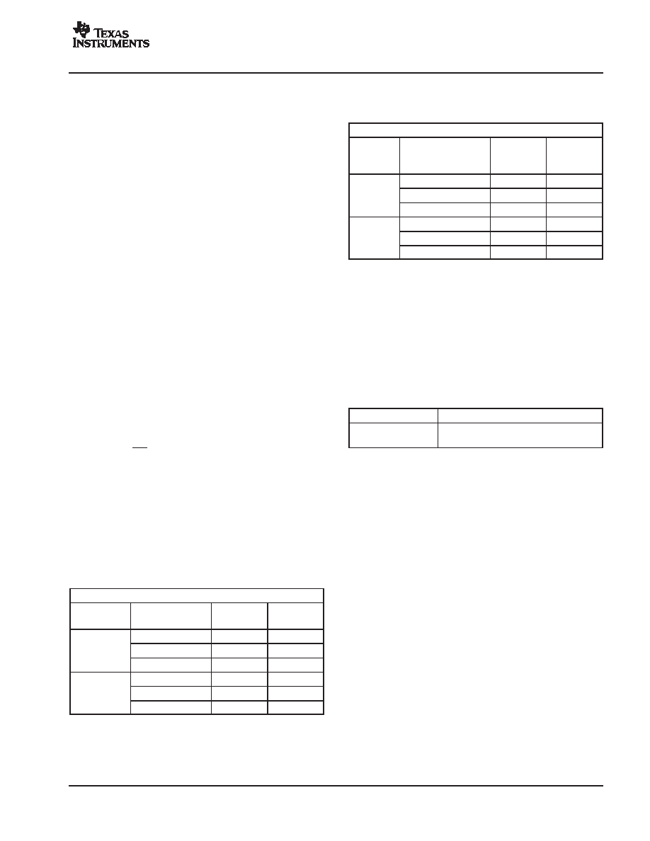
POWER-DOWN THRESHOLD VOLTAGE LEVELS (REF
≤ MIDRAIL)
SUPPLY
REFERENCE PIN
ENABLE
DISABLE
SUPPLY
VOLTAGE(V)
REFERENCE PIN
VOLTAGE (V)
ENABLE
LEVEL (V)
DISABLE
LEVEL (V)
GND
≥ 1.8
≤ 1
±5
2.5
≥ 0.7
≤ 1.5
±5
5
≥ 3.2
≤ 4
GND
≥ 1.8
≤ 1
5
1
≥ 2.8
≤ 2
5
2.5
≥ 4.3
≤ 3.5
In the above table, the threshold levels are derived by the
following equations:
REF + 1.8 V for enable
REF + 1 V for disable
Note that in order to maintain these threshold levels, the
reference pin can be any voltage between Vs or GND up
to Vs/2 (midrail).
POWER-DOWN THRESHOLD VOLTAGE LEVELS (REF > MIDRAIL)
SUPPLY
VOLTAGE
REFERENCE PIN
ENABLE
DISABLE
VOLTAGE
(V)
REFERENCE PIN
VOLTAGE (V)
ENABLE
LEVEL (V)
DISABLE
LEVEL (V)
Floating or 5
≥ 4
≤ 3.3
±5
2.5
≥ 1.5
≤ 0.8
±5
1
≥ 0
≤ 0.7
Floating or 5
≥ 3.3
≤ 3.3
5
4
≥ 3
≤ 2.3
5
3.5
≥ 2.5
≤ 1.8
In the above table, the threshold levels are derived by the
following equations:
REF 1 V for enable
REF 1.7 V for disable
Note that in order to maintain these threshold levels, the
reference pin can be any voltage between (Vs+/2) + 1 V to
Vs+.
The recommended mode of operation is to tie the
reference pin to midrail, thus setting the threshold levels to
midrail +1 V and midrail +1.8 V.
NO. OF CHANNELS
PACKAGES
Single (8 pin)
THS4275D, THS4275DGN, and
THS4275DRB
Power Supply Decoupling Techniques and
Recommendations
Power supply decoupling is a critical aspect of any
high-performance amplifier design process. Careful
decoupling provides higher quality ac performance (most
notably improved distortion performance). The following
guidelines ensure the highest level of performance.
1.
Place decoupling capacitors as close to the power
supply inputs as possible, with the goal of minimizing
the inductance of the path from ground to the power
supply.
2.
Placement priority should put the smallest valued
capacitors closest to the device.
3.
Use
of
solid
power
and
ground
planes
is
recommended to reduce the inductance along power
supply return current paths, with the exception of the
areas underneath the input and output pins.
4.
Recommended values for power supply decoupling
include a bulk decoupling capacitor (6.8 to 22
F), a
mid-range decoupling capacitor (0.1
F) and a high
frequency decoupling capacitor (1000 pF) for each
supply. A 100-pF capacitor can be used across the
supplies as well for extremely high frequency return
currents, but often is not required.
相关PDF资料 |
PDF描述 |
|---|---|
| THS4271MDREPR | 1 CHANNEL, VIDEO AMPLIFIER, PDSO8 |
| THS4271MDGNTEPR | 1 CHANNEL, VIDEO AMPLIFIER, PDSO8 |
| THS4271MDEPR | 1 CHANNEL, VIDEO AMPLIFIER, PDSO8 |
| THS4275MDEPR | 1 CHANNEL, VIDEO AMPLIFIER, PDSO8 |
| THS4275MDREPR | 1 CHANNEL, VIDEO AMPLIFIER, PDSO8 |
相关代理商/技术参数 |
参数描述 |
|---|---|
| THS4281 | 制造商:TI 制造商全称:Texas Instruments 功能描述:VERY LOW-POWER, HIGH-SPEED, RAIL-TO-RAIL INPUT AND OUTPUT VOLTAGE-FEEDBACK OPERATIONAL AMPLIFIER |
| THS4281D | 功能描述:高速运算放大器 Very Lo-Pwr R-To-R I/O Voltage Feedback RoHS:否 制造商:Texas Instruments 通道数量:1 电压增益 dB:116 dB 输入补偿电压:0.5 mV 转换速度:55 V/us 工作电源电压:36 V 电源电流:7.5 mA 最大工作温度:+ 85 C 安装风格:SMD/SMT 封装 / 箱体:SOIC-8 封装:Tube |
| THS4281DBVR | 功能描述:高速运算放大器 Very Lo-Pwr R-To-R I/O Voltage Feedback RoHS:否 制造商:Texas Instruments 通道数量:1 电压增益 dB:116 dB 输入补偿电压:0.5 mV 转换速度:55 V/us 工作电源电压:36 V 电源电流:7.5 mA 最大工作温度:+ 85 C 安装风格:SMD/SMT 封装 / 箱体:SOIC-8 封装:Tube |
| THS4281DBVRG4 | 功能描述:高速运算放大器 Very Lo-Pwr R-To-R I/O Voltage Feedback RoHS:否 制造商:Texas Instruments 通道数量:1 电压增益 dB:116 dB 输入补偿电压:0.5 mV 转换速度:55 V/us 工作电源电压:36 V 电源电流:7.5 mA 最大工作温度:+ 85 C 安装风格:SMD/SMT 封装 / 箱体:SOIC-8 封装:Tube |
| THS4281DBVT | 功能描述:高速运算放大器 Very Lo-Pwr R-To-R I/O Voltage Feedback RoHS:否 制造商:Texas Instruments 通道数量:1 电压增益 dB:116 dB 输入补偿电压:0.5 mV 转换速度:55 V/us 工作电源电压:36 V 电源电流:7.5 mA 最大工作温度:+ 85 C 安装风格:SMD/SMT 封装 / 箱体:SOIC-8 封装:Tube |
发布紧急采购,3分钟左右您将得到回复。