- 您现在的位置:买卖IC网 > PDF目录98227 > THS4281DG4 (TEXAS INSTRUMENTS INC) 1 CHANNEL, VIDEO AMPLIFIER, PDSO8 PDF资料下载
参数资料
| 型号: | THS4281DG4 |
| 厂商: | TEXAS INSTRUMENTS INC |
| 元件分类: | 音频/视频放大 |
| 英文描述: | 1 CHANNEL, VIDEO AMPLIFIER, PDSO8 |
| 封装: | GREEN, PLASTIC, SOIC-8 |
| 文件页数: | 10/37页 |
| 文件大小: | 1063K |
| 代理商: | THS4281DG4 |
第1页第2页第3页第4页第5页第6页第7页第8页第9页当前第10页第11页第12页第13页第14页第15页第16页第17页第18页第19页第20页第21页第22页第23页第24页第25页第26页第27页第28页第29页第30页第31页第32页第33页第34页第35页第36页第37页
_
+
Rf
2.49 k
49.9
0.1
F 6.8 F
VS
Rg
50-
Source
+
VI
0.1
F 6.8 F
+
+VS
VO
2.49 k
To Load
0
4
8
12
16
20
24
0.1
1
10
100
VS = 3 V
Gain = 10,
RL = 1 k,
VO = 0.1 VPP
RF = 100 k
f Frequency MHz
RF = 1.65 k
and 10 k
Signal
Gain
dB
0
4
8
12
16
20
24
0.1
1
10
100
VS = ±5 V
Gain = 10,
RL = 1 k,
VO = 0.1 VPP
RF = 100 k
f Frequency MHz
RF = 2.5 k
and 10 k
Signal
Gain
dB
SLOS432A – APRIL 2004 – REVISED NOVEMBER 2009
www.ti.com
APPLICATION INFORMATION
HIGH-SPEED OPERATIONAL AMPLIFIERS
The THS4281 is a unity gain stable, rail-to-rail input
and output, voltage-feedback operational amplifier
designed to operate from a single 2.7-V to 16.5-V
power supply.
Applications Section Contents
Wideband, Noninverting Operation
Wideband, Inverting Gain Operation
Video Drive Circuits
Single-Supply Operation
Power-Supply
Decoupling
Techniques
and
Recommendations
Active Filtering with the THS4281
Driving Capacitive Loads
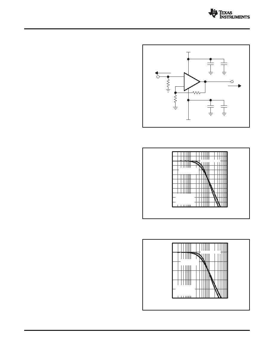
Figure 68. Wideband, Noninverting Gain
Board Layout
Configuration
Thermal Analysis
Additional Reference Material
Mechanical Package Drawings
WIDEBAND, NONINVERTING OPERATION
Figure 68 shows the noninverting gain configuration
of 2 V/V used to demonstrate the typical performance
curves.
Voltage feedback amplifiers can use a wide range of
resistors values to set their gain with minimal impact
on
frequency
response.
Larger-valued
resistors
decrease loading of the feedback network on the
output of the amplifier, but may cause peaking and
instability. For a gain of +2, feedback resistor values
between 1 k
and 4 k are recommended for most
applications. However, as the gain increases, the use
Figure 69. Signal Gain vs
of even higher feedback resistors can be used to
Frequency, VS = 3 V
conserve power. This is due to the inherent nature of
amplifiers
becoming
more
stable
as
the
gain
increases, at the expense of bandwidth. Figure 69
and Figure 70 show the THS4281 using feedback
resistors of 10 k
and 100 k. Be cautioned that
using such high values with high-speed amplifiers is
not
typically
recommended,
but
under
certain
conditions, such as high gain and good high-speed
printed circuit board (PCB) layout practices, such
resistances can be used.
Figure 70. Signal Gain vs
Frequency, VS = ±5 V
18
Copyright 2004–2009, Texas Instruments Incorporated
Product Folder Link(s): THS4281
相关PDF资料 |
PDF描述 |
|---|---|
| THS4281DBVR | 1 CHANNEL, VIDEO AMPLIFIER, PDSO5 |
| THS4281DBVT | 1 CHANNEL, VIDEO AMPLIFIER, PDSO5 |
| THS4281DGKR | 1 CHANNEL, VIDEO AMPLIFIER, PDSO8 |
| THS4281DGK | 1 CHANNEL, VIDEO AMPLIFIER, PDSO8 |
| THS4281DR | 1 CHANNEL, VIDEO AMPLIFIER, PDSO8 |
相关代理商/技术参数 |
参数描述 |
|---|---|
| THS4281DGK | 功能描述:高速运算放大器 Very Lo-Pwr R-To-R I/O Voltage Feedback RoHS:否 制造商:Texas Instruments 通道数量:1 电压增益 dB:116 dB 输入补偿电压:0.5 mV 转换速度:55 V/us 工作电源电压:36 V 电源电流:7.5 mA 最大工作温度:+ 85 C 安装风格:SMD/SMT 封装 / 箱体:SOIC-8 封装:Tube |
| THS4281DGKG4 | 功能描述:高速运算放大器 Very Lo-Pwr R-To-R I/O Voltage Feedback RoHS:否 制造商:Texas Instruments 通道数量:1 电压增益 dB:116 dB 输入补偿电压:0.5 mV 转换速度:55 V/us 工作电源电压:36 V 电源电流:7.5 mA 最大工作温度:+ 85 C 安装风格:SMD/SMT 封装 / 箱体:SOIC-8 封装:Tube |
| THS4281DGKR | 功能描述:高速运算放大器 Very Lo-Pwr R-To-R I/O Voltage Feedback RoHS:否 制造商:Texas Instruments 通道数量:1 电压增益 dB:116 dB 输入补偿电压:0.5 mV 转换速度:55 V/us 工作电源电压:36 V 电源电流:7.5 mA 最大工作温度:+ 85 C 安装风格:SMD/SMT 封装 / 箱体:SOIC-8 封装:Tube |
| THS4281DGKRG4 | 功能描述:高速运算放大器 Very Lo-Pwr R-To-R I/O Voltage Feedback RoHS:否 制造商:Texas Instruments 通道数量:1 电压增益 dB:116 dB 输入补偿电压:0.5 mV 转换速度:55 V/us 工作电源电压:36 V 电源电流:7.5 mA 最大工作温度:+ 85 C 安装风格:SMD/SMT 封装 / 箱体:SOIC-8 封装:Tube |
| THS4281DR | 功能描述:高速运算放大器 Very Lo-Pwr R-To-R I/O Voltage Feedback RoHS:否 制造商:Texas Instruments 通道数量:1 电压增益 dB:116 dB 输入补偿电压:0.5 mV 转换速度:55 V/us 工作电源电压:36 V 电源电流:7.5 mA 最大工作温度:+ 85 C 安装风格:SMD/SMT 封装 / 箱体:SOIC-8 封装:Tube |
发布紧急采购,3分钟左右您将得到回复。