- 您现在的位置:买卖IC网 > PDF目录98227 > THS4281DG4 (TEXAS INSTRUMENTS INC) 1 CHANNEL, VIDEO AMPLIFIER, PDSO8 PDF资料下载
参数资料
| 型号: | THS4281DG4 |
| 厂商: | TEXAS INSTRUMENTS INC |
| 元件分类: | 音频/视频放大 |
| 英文描述: | 1 CHANNEL, VIDEO AMPLIFIER, PDSO8 |
| 封装: | GREEN, PLASTIC, SOIC-8 |
| 文件页数: | 15/37页 |
| 文件大小: | 1063K |
| 代理商: | THS4281DG4 |
第1页第2页第3页第4页第5页第6页第7页第8页第9页第10页第11页第12页第13页第14页当前第15页第16页第17页第18页第19页第20页第21页第22页第23页第24页第25页第26页第27页第28页第29页第30页第31页第32页第33页第34页第35页第36页第37页
P
Dmax +
Tmax–TA
q
JA
where:
PDmax is the maximum power dissipation in the amplifier (W).
Tmax is the absolute maximum junction temperature (°C).
TA is the ambient temperature (°C).
θJA = θJC + θCA
θJC is the thermal coefficient from the silicon junctions to the
case (
°C/W).
θCA is the thermal coefficient from the case to ambient air
(
°C/W).
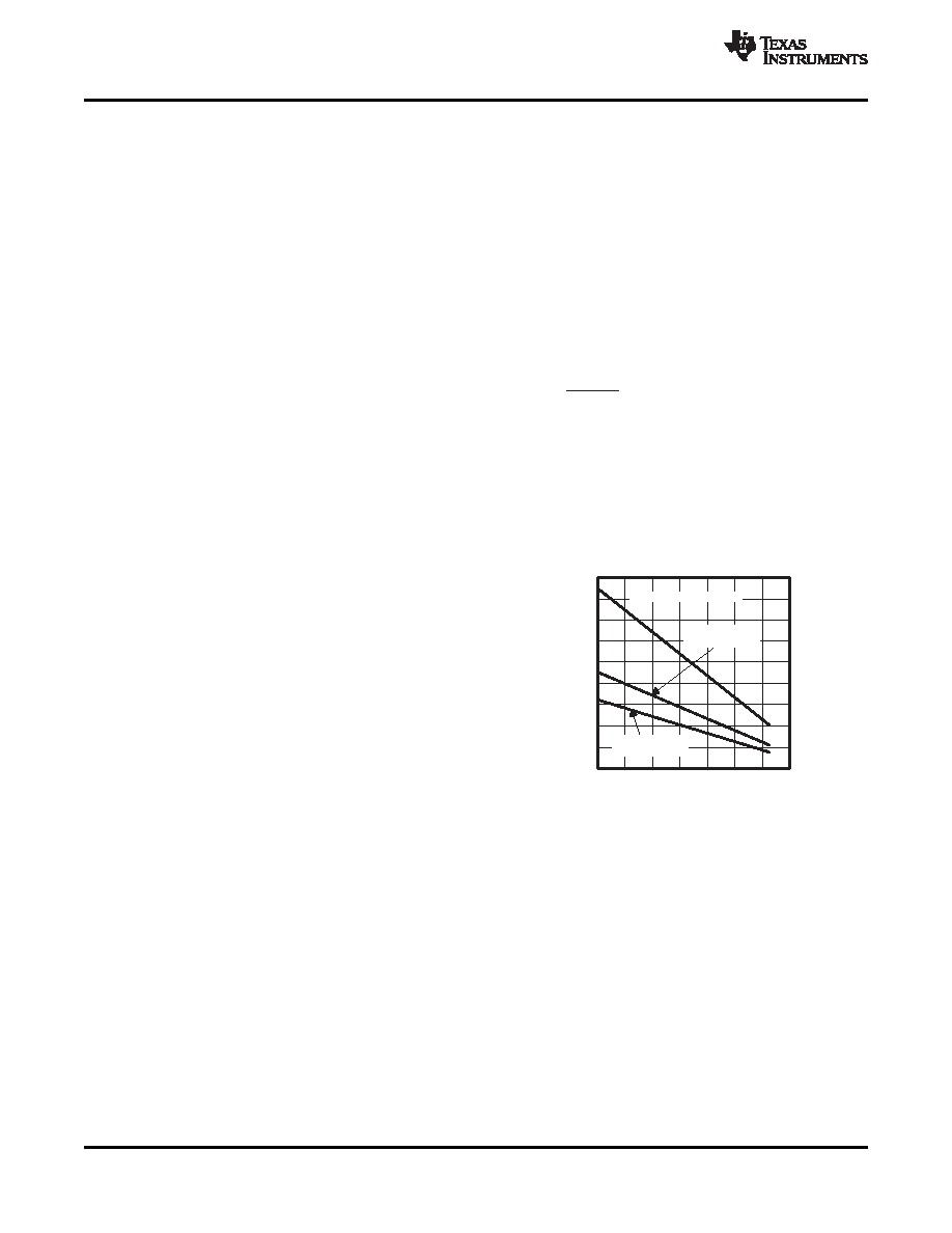
0
0.2
0.4
0.6
0.8
1
1.2
1.4
1.6
1.8
40
20
0
20
40
60
80
100
8-pin SOIC (D) Package
8-pin MSOP
(DGK) Package
5-pin SOT23
(DBV) Package
Maximum
Power
Dissipation
W
P
D
TA Free-Air Temperature °C
θJA = 97.5°C/W for 8-Pin SOIC (D)
θJA = 180.8°C/W for 8-Pin MSOP (DGK)
θJA = 255.4°C/W for 5-Pin SOT23 (DBV)
TJ = 125°C, No Airflow
SLOS432A – APRIL 2004 – REVISED NOVEMBER 2009
www.ti.com
4. Connections to other wideband devices on
THERMAL ANALYSIS
the board should be made with short direct
The THS4281 does not incorporate automatic thermal
traces or through onboard transmission lines.
shutoff protection, so the designer must take care to
For short connections, consider the trace and the
ensure that the design does not violate the absolute
input to the next device as a lumped capacitive
maximum junction temperature of the device. Failure
load. Relatively wide traces (50 mils to 100 mils)
may
result
if
the
absolute
maximum
junction
should be used, preferably with ground and
temperature of +150° C is exceeded. For long-term
power planes opened up around them. Low
dependability, the junction temperature should not
parasitic capacitive loads (< 4 pF) may not need
exceed +125°C.
an R(ISO), because the THS4281 is nominally
compensated to operate at unity gain (+1 V/V)
The thermal characteristics of the device are dictated
with a 2-pF capacitive load. Higher capacitive
by the package and the PCB. Maximum power
loads without an R(ISO) are allowed as the signal
dissipation for a given package can be calculated
gain increases. If a long trace is required, and the
using the following formula.
6-dB signal loss intrinsic to a doubly terminated
transmission line is acceptable, implement a
matched
impedance
transmission
line
using
microstrip or stripline techniques (consult an ECL
design handbook for microstrip and stripline
layout techniques). A matching series resistor into
the trace from the output of the THS4281 is used
as well as a terminating shunt resistor at the input
of the destination device. Remember also that the
terminating impedance is the parallel combination
of the shunt resistor and the input impedance of
the
destination
device:
this
total
effective
impedance should be set to match the trace
impedance.
If
the
6-dB
attenuation
of
a
doubly-terminated
transmission
line
is
unacceptable,
a
long
trace
can
be
series-terminated at the source end only. Treat
the trace as a capacitive load in this case, and
use a series resistor (R(ISO) = 10 Ω to 100 Ω, as
noted above) to isolate the capacitive load. If the
input impedance of the destination device is low,
there is signal attenuation due to the voltage
divider formed by R(ISO) into the terminating
impedance. A 50-
environment is normally not
necessary
onboard,
and
in
fact
a
higher
impedance environment improves distortion as
shown in the distortion versus load plots.
5. Socketing a high-speed part like the THS4281
is not recommended. The additional lead length
and pin-to-pin capacitance introduced by the
Figure 76. Maximum Power Dissipation vs
socket
can
create
a
troublesome
parasitic
Ambient Temperature
network which can make it almost impossible to
achieve a smooth, stable frequency response.
When determining whether or not the device satisfies
Best results are obtained by soldering the
the maximum power dissipation requirement, it is
THS4281 onto the board.
important to consider not only quiescent power
space
dissipation, but also dynamic power dissipation. Often
maximum power dissipation is difficult to quantify
space
because the signal pattern is inconsistent, but an
estimate of the RMS value can provide a reasonable
analysis.
22
Copyright 2004–2009, Texas Instruments Incorporated
Product Folder Link(s): THS4281
相关PDF资料 |
PDF描述 |
|---|---|
| THS4281DBVR | 1 CHANNEL, VIDEO AMPLIFIER, PDSO5 |
| THS4281DBVT | 1 CHANNEL, VIDEO AMPLIFIER, PDSO5 |
| THS4281DGKR | 1 CHANNEL, VIDEO AMPLIFIER, PDSO8 |
| THS4281DGK | 1 CHANNEL, VIDEO AMPLIFIER, PDSO8 |
| THS4281DR | 1 CHANNEL, VIDEO AMPLIFIER, PDSO8 |
相关代理商/技术参数 |
参数描述 |
|---|---|
| THS4281DGK | 功能描述:高速运算放大器 Very Lo-Pwr R-To-R I/O Voltage Feedback RoHS:否 制造商:Texas Instruments 通道数量:1 电压增益 dB:116 dB 输入补偿电压:0.5 mV 转换速度:55 V/us 工作电源电压:36 V 电源电流:7.5 mA 最大工作温度:+ 85 C 安装风格:SMD/SMT 封装 / 箱体:SOIC-8 封装:Tube |
| THS4281DGKG4 | 功能描述:高速运算放大器 Very Lo-Pwr R-To-R I/O Voltage Feedback RoHS:否 制造商:Texas Instruments 通道数量:1 电压增益 dB:116 dB 输入补偿电压:0.5 mV 转换速度:55 V/us 工作电源电压:36 V 电源电流:7.5 mA 最大工作温度:+ 85 C 安装风格:SMD/SMT 封装 / 箱体:SOIC-8 封装:Tube |
| THS4281DGKR | 功能描述:高速运算放大器 Very Lo-Pwr R-To-R I/O Voltage Feedback RoHS:否 制造商:Texas Instruments 通道数量:1 电压增益 dB:116 dB 输入补偿电压:0.5 mV 转换速度:55 V/us 工作电源电压:36 V 电源电流:7.5 mA 最大工作温度:+ 85 C 安装风格:SMD/SMT 封装 / 箱体:SOIC-8 封装:Tube |
| THS4281DGKRG4 | 功能描述:高速运算放大器 Very Lo-Pwr R-To-R I/O Voltage Feedback RoHS:否 制造商:Texas Instruments 通道数量:1 电压增益 dB:116 dB 输入补偿电压:0.5 mV 转换速度:55 V/us 工作电源电压:36 V 电源电流:7.5 mA 最大工作温度:+ 85 C 安装风格:SMD/SMT 封装 / 箱体:SOIC-8 封装:Tube |
| THS4281DR | 功能描述:高速运算放大器 Very Lo-Pwr R-To-R I/O Voltage Feedback RoHS:否 制造商:Texas Instruments 通道数量:1 电压增益 dB:116 dB 输入补偿电压:0.5 mV 转换速度:55 V/us 工作电源电压:36 V 电源电流:7.5 mA 最大工作温度:+ 85 C 安装风格:SMD/SMT 封装 / 箱体:SOIC-8 封装:Tube |
发布紧急采购,3分钟左右您将得到回复。