- 您现在的位置:买卖IC网 > PDF目录299979 > TLC071AIPE4 (TEXAS INSTRUMENTS INC) OP-AMP, 2000 uV OFFSET-MAX, 10 MHz BAND WIDTH, PDIP8 PDF资料下载
参数资料
| 型号: | TLC071AIPE4 |
| 厂商: | TEXAS INSTRUMENTS INC |
| 元件分类: | 运算放大器 |
| 英文描述: | OP-AMP, 2000 uV OFFSET-MAX, 10 MHz BAND WIDTH, PDIP8 |
| 封装: | ROHS COMPLIANT, PLASTIC, DIP-8 |
| 文件页数: | 17/53页 |
| 文件大小: | 1664K |
| 代理商: | TLC071AIPE4 |
第1页第2页第3页第4页第5页第6页第7页第8页第9页第10页第11页第12页第13页第14页第15页第16页当前第17页第18页第19页第20页第21页第22页第23页第24页第25页第26页第27页第28页第29页第30页第31页第32页第33页第34页第35页第36页第37页第38页第39页第40页第41页第42页第43页第44页第45页第46页第47页第48页第49页第50页第51页第52页第53页
TLC070, TLC071, TLC072, TLC073, TLC074, TLC075, TLC07xA
FAMILY OF WIDEBANDWIDTH HIGHOUTPUT DRIVE SINGLE SUPPLY
OPERATIONAL AMPLIFIERS
SLOS219E JUNE 1999 REVISED SEPTEMBER 2006
24
WWW.TI.COM
POST OFFICE BOX 1443
HOUSTON, TEXAS 772511443
APPLICATION INFORMATION
general PowerPAD design considerations (continued)
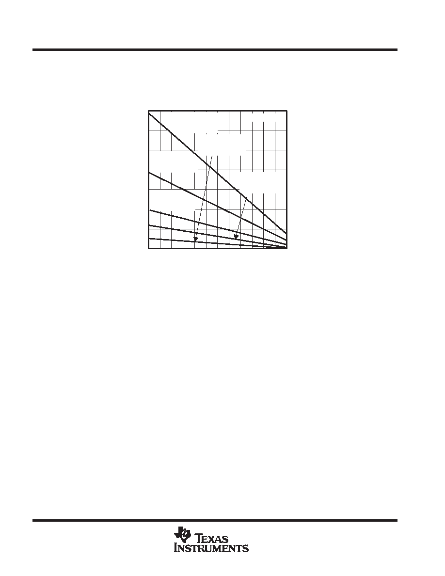
TJ = 150°C
4
3
2
0
55 40
10
20 35
Maximum
Power
Dissipation
W
5
6
MAXIMUM POWER DISSIPATION
vs
FREE-AIR TEMPERATURE
7
65
95
125
1
TA Free-Air Temperature °C
DGN Package
Low-K Test PCB
θJA = 52.3°C/W
SOT-23 Package
Low-K Test PCB
θJA = 324°C/W
25
5
50
80
110
PWP Package
Low-K Test PCB
θJA = 29.7°C/W
SOIC Package
Low-K Test PCB
θJA = 176°C/W
PDIP Package
Low-K Test PCB
θJA = 104°C/W
NOTE A: Results are with no air flow and using JEDEC Standard Low-K test PCB.
Figure 53. Maximum Power Dissipation vs Free-Air Temperature
The next consideration is the package constraints. The two sources of heat within an amplifier are quiescent
power and output power. The designer should never forget about the quiescent heat generated within the
device, especially multi-amplifier devices. Because these devices have linear output stages (Class A-B), most
of the heat dissipation is at low output voltages with high output currents.
The other key factor when dealing with power dissipation is how the devices are mounted on the PCB. The
PowerPAD devices are extremely useful for heat dissipation. But, the device should always be soldered to a
copper plane to fully use the heat dissipation properties of the PowerPAD. The SOIC package, on the other
hand, is highly dependent on how it is mounted on the PCB. As more trace and copper area is placed around
the device,
θJA decreases and the heat dissipation capability increases. The currents and voltages shown in
these graphs are for the total package. For the dual or quad amplifier packages, the sum of the RMS output
currents and voltages should be used to choose the proper package.
相关PDF资料 |
PDF描述 |
|---|---|
| TLC251ACDRG4 | OP-AMP, 6500 uV OFFSET-MAX, 1.7 MHz BAND WIDTH, PDSO8 |
| TLE7719-T | SPECIALTY ANALOG CIRCUIT, PDSO28 |
| TLH124C | RF/MICROWAVE DOWN CONVERTER |
| TLOM1060(T18) | SINGLE COLOR LED, ORANGE |
| TLP2403(F) | 1 CHANNEL LOGIC OUTPUT OPTOCOUPLER |
相关代理商/技术参数 |
参数描述 |
|---|---|
| TLC071CD | 功能描述:运算放大器 - 运放 High Speed R/R RoHS:否 制造商:STMicroelectronics 通道数量:4 共模抑制比(最小值):63 dB 输入补偿电压:1 mV 输入偏流(最大值):10 pA 工作电源电压:2.7 V to 5.5 V 安装风格:SMD/SMT 封装 / 箱体:QFN-16 转换速度:0.89 V/us 关闭:No 输出电流:55 mA 最大工作温度:+ 125 C 封装:Reel |
| TLC071CD | 制造商:Texas Instruments 功能描述:OP AMP HI SPEED RRIO SMD SOIC8 |
| TLC071CDG4 | 功能描述:运算放大器 - 运放 Sngl Wide-Bandwidth Hi-Output-Drv Op Amp RoHS:否 制造商:STMicroelectronics 通道数量:4 共模抑制比(最小值):63 dB 输入补偿电压:1 mV 输入偏流(最大值):10 pA 工作电源电压:2.7 V to 5.5 V 安装风格:SMD/SMT 封装 / 箱体:QFN-16 转换速度:0.89 V/us 关闭:No 输出电流:55 mA 最大工作温度:+ 125 C 封装:Reel |
| TLC071CDGN | 功能描述:运算放大器 - 运放 Sngl Wide-Bandwidth Hi-Output-Drv Op Amp RoHS:否 制造商:STMicroelectronics 通道数量:4 共模抑制比(最小值):63 dB 输入补偿电压:1 mV 输入偏流(最大值):10 pA 工作电源电压:2.7 V to 5.5 V 安装风格:SMD/SMT 封装 / 箱体:QFN-16 转换速度:0.89 V/us 关闭:No 输出电流:55 mA 最大工作温度:+ 125 C 封装:Reel |
| TLC071CDGNG4 | 功能描述:运算放大器 - 运放 Sngl Wide-Bandwidth Hi-Output-Drv Op Amp RoHS:否 制造商:STMicroelectronics 通道数量:4 共模抑制比(最小值):63 dB 输入补偿电压:1 mV 输入偏流(最大值):10 pA 工作电源电压:2.7 V to 5.5 V 安装风格:SMD/SMT 封装 / 箱体:QFN-16 转换速度:0.89 V/us 关闭:No 输出电流:55 mA 最大工作温度:+ 125 C 封装:Reel |
发布紧急采购,3分钟左右您将得到回复。