- 您现在的位置:买卖IC网 > PDF目录67339 > TLV1543CDBR (TEXAS INSTRUMENTS INC) 11-CH 10-BIT SUCCESSIVE APPROXIMATION ADC, SERIAL ACCESS, PDSO20 PDF资料下载
参数资料
| 型号: | TLV1543CDBR |
| 厂商: | TEXAS INSTRUMENTS INC |
| 元件分类: | ADC |
| 英文描述: | 11-CH 10-BIT SUCCESSIVE APPROXIMATION ADC, SERIAL ACCESS, PDSO20 |
| 封装: | GREEN, PLASTIC, SSOP-20 |
| 文件页数: | 23/29页 |
| 文件大小: | 804K |
| 代理商: | TLV1543CDBR |
第1页第2页第3页第4页第5页第6页第7页第8页第9页第10页第11页第12页第13页第14页第15页第16页第17页第18页第19页第20页第21页第22页当前第23页第24页第25页第26页第27页第28页第29页
TLV1543C, TLV1543I, TLV1543M
3.3V 10BIT ANALOGTODIGITAL CONVERTERS
WITH SERIAL CONTROL AND 11 ANALOG INPUTS
SLAS072E DECEMBER 1992 REVISED JANUARY 2004
3
WWW.TI.COM
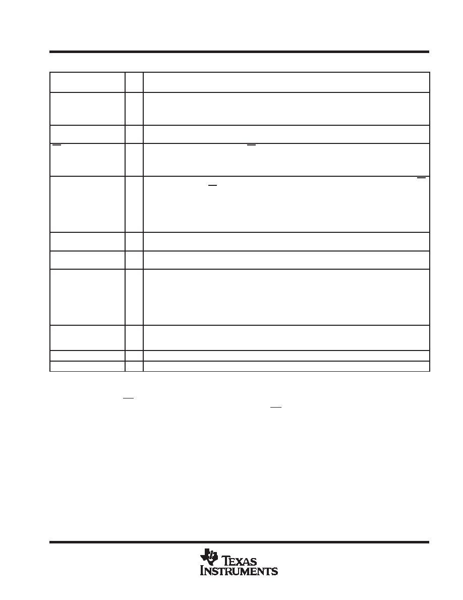
Terminal Functions
TERMINAL
I/O
DESCRIPTION
NAME
NO.
I/O
DESCRIPTION
ADDRESS
17
I
Serial address. A 4-bit serial address selects the desired analog input or test voltage that is to be converted
next. The address data is presented with the MSB first and is shifted in on the first four rising edges of I/O
CLOCK. After the four address bits have been read into the address register, ADDRESS is ignored for the
remainder of the current conversion period.
A0 A10
1 9, 11,
12
I
Analog signal. The 11 analog inputs are applied to A0 A10 and are internally multiplexed. The driving source
impedance should be less than or equal to 1 k
.
CS
15
I
Chip select. A high-to-low transition on CS resets the internal counters and controls and enables DATA OUT,
ADDRESS, and I/O CLOCK within a maximum of a setup time plus two falling edges of the internal system
clock. A low-to-high transition disables ADDRESS and I/O CLOCK within a setup time plus two falling edges
of the internal system clock.
DATA OUT
16
O
The 3-state serial output for the A/D conversion result. DATA OUT is in the high-impedance state when CS
is high and active when CS is low. With a valid chip select, DATA OUT is removed from the high-impedance
state and is driven to the logic level corresponding to the MSB value of the previous conversion result. The
next falling edge of I/O CLOCK drives DATA OUT to the logic level corresponding to the next most significant
bit, and the remaining bits are shifted out in order with the LSB appearing on the ninth falling edge of I/O
CLOCK. On the tenth falling edge of I/O CLOCK, DATA OUT is driven to a low logic level so that serial
interface data transfers of more than ten clocks produce zeroes as the unused LSBs.
EOC
19
O
End of conversion. EOC goes from a high- to a low- logic level on the trailing edge of the tenth I/O CLOCK
and remains low until the conversion is complete and data are ready for transfer.
GND
10
I
The ground return terminal for the internal circuitry. Unless otherwise noted, all voltage measurements are
with respect to GND.
I/O CLOCK
18
I
Input/output clock. I/O CLOCK receives the serial I/O CLOCK input and performs the following four functions:
1) It clocks the four input address bits into the address register on the first four rising edges of I/O
CLOCK with the multiplex address available after the fourth rising edge.
2) On the fourth falling edge of I/O CLOCK, the analog input voltage on the selected multiplex input begins
charging the capacitor array and continues to do so until the tenth falling edge of I/O CLOCK.
3) It shifts the nine remaining bits of the previous conversion data out on DATA OUT.
4) It transfers control of the conversion to the internal state controller on the falling edge of the tenth clock.
REF +
14
I
The upper reference voltage value (nominally VCC) is applied to REF +. The maximum input voltage range
is determined by the difference between the voltage applied to REF + and the voltage applied to the REF
terminal.
REF
13
I
The lower reference voltage value (nominally ground) is applied to REF .
VCC
20
I
Positive supply voltage
detailed description
With chip select (CS) inactive (high), the ADDRESS and I/O CLOCK inputs are initially disabled and DATA OUT
is in the high-impedance state. When the serial interface takes CS active (low), the conversion sequence begins
with the enabling of I/O CLOCK and ADDRESS and the removal of DATA OUT from the high-impedance state.
The host then provides the 4-bit channel address to ADDRESS and the I/O CLOCK sequence to I/O CLOCK.
During this transfer, the host serial interface also receives the previous conversion result from DATA OUT. I/O
CLOCK receives an input sequence that is between 10 and 16 clocks long from the host. The first four I/O clocks
load the address register with the 4-bit address on ADDRESS selecting the desired analog channel and the next
six clocks providing the control timing for sampling the analog input.
相关PDF资料 |
PDF描述 |
|---|---|
| TLV1543CDBG4 | 11-CH 10-BIT SUCCESSIVE APPROXIMATION ADC, SERIAL ACCESS, PDSO20 |
| TLV1543CDBRG4 | 11-CH 10-BIT SUCCESSIVE APPROXIMATION ADC, SERIAL ACCESS, PDSO20 |
| TLV1543CFN | 11-CH 10-BIT SUCCESSIVE APPROXIMATION ADC, SERIAL ACCESS, PQCC20 |
| TLV1543IDB | 11-CH 10-BIT SUCCESSIVE APPROXIMATION ADC, SERIAL ACCESS, PDSO20 |
| TLV1543CN | 11-CH 10-BIT SUCCESSIVE APPROXIMATION ADC, SERIAL ACCESS, PDIP20 |
相关代理商/技术参数 |
参数描述 |
|---|---|
| TLV1543CDBRG4 | 功能描述:模数转换器 - ADC 10-Bit 200 kSPS Serial Out RoHS:否 制造商:Texas Instruments 通道数量:2 结构:Sigma-Delta 转换速率:125 SPs to 8 KSPs 分辨率:24 bit 输入类型:Differential 信噪比:107 dB 接口类型:SPI 工作电源电压:1.7 V to 3.6 V, 2.7 V to 5.25 V 最大工作温度:+ 85 C 安装风格:SMD/SMT 封装 / 箱体:VQFN-32 |
| TLV1543CDW | 功能描述:模数转换器 - ADC 10bit ADC w/11Chl RoHS:否 制造商:Texas Instruments 通道数量:2 结构:Sigma-Delta 转换速率:125 SPs to 8 KSPs 分辨率:24 bit 输入类型:Differential 信噪比:107 dB 接口类型:SPI 工作电源电压:1.7 V to 3.6 V, 2.7 V to 5.25 V 最大工作温度:+ 85 C 安装风格:SMD/SMT 封装 / 箱体:VQFN-32 |
| TLV1543CDWG4 | 功能描述:模数转换器 - ADC 10-Bit 200 kSPS Serial Out RoHS:否 制造商:Texas Instruments 通道数量:2 结构:Sigma-Delta 转换速率:125 SPs to 8 KSPs 分辨率:24 bit 输入类型:Differential 信噪比:107 dB 接口类型:SPI 工作电源电压:1.7 V to 3.6 V, 2.7 V to 5.25 V 最大工作温度:+ 85 C 安装风格:SMD/SMT 封装 / 箱体:VQFN-32 |
| TLV1543CDWR | 功能描述:模数转换器 - ADC 10-Bit 200 kSPS Serial Out RoHS:否 制造商:Texas Instruments 通道数量:2 结构:Sigma-Delta 转换速率:125 SPs to 8 KSPs 分辨率:24 bit 输入类型:Differential 信噪比:107 dB 接口类型:SPI 工作电源电压:1.7 V to 3.6 V, 2.7 V to 5.25 V 最大工作温度:+ 85 C 安装风格:SMD/SMT 封装 / 箱体:VQFN-32 |
| TLV1543CDWRG4 | 功能描述:模数转换器 - ADC 10-Bit 200 kSPS Serial Out RoHS:否 制造商:Texas Instruments 通道数量:2 结构:Sigma-Delta 转换速率:125 SPs to 8 KSPs 分辨率:24 bit 输入类型:Differential 信噪比:107 dB 接口类型:SPI 工作电源电压:1.7 V to 3.6 V, 2.7 V to 5.25 V 最大工作温度:+ 85 C 安装风格:SMD/SMT 封装 / 箱体:VQFN-32 |
发布紧急采购,3分钟左右您将得到回复。