- 您现在的位置:买卖IC网 > PDF目录67339 > TLV1543CDBR (TEXAS INSTRUMENTS INC) 11-CH 10-BIT SUCCESSIVE APPROXIMATION ADC, SERIAL ACCESS, PDSO20 PDF资料下载
参数资料
| 型号: | TLV1543CDBR |
| 厂商: | TEXAS INSTRUMENTS INC |
| 元件分类: | ADC |
| 英文描述: | 11-CH 10-BIT SUCCESSIVE APPROXIMATION ADC, SERIAL ACCESS, PDSO20 |
| 封装: | GREEN, PLASTIC, SSOP-20 |
| 文件页数: | 24/29页 |
| 文件大小: | 804K |
| 代理商: | TLV1543CDBR |
第1页第2页第3页第4页第5页第6页第7页第8页第9页第10页第11页第12页第13页第14页第15页第16页第17页第18页第19页第20页第21页第22页第23页当前第24页第25页第26页第27页第28页第29页
TLV1543C, TLV1543I, TLV1543M
3.3V 10BIT ANALOGTODIGITAL CONVERTERS
WITH SERIAL CONTROL AND 11 ANALOG INPUTS
SLAS072E DECEMBER 1992 REVISED JANUARY 2004
4
WWW.TI.COM
detailed description (continued)
There are six basic serial interface timing modes that can be used with the device. These modes are determined
by the speed of I/O CLOCK and the operation of CS as shown in Table 1. These modes are (1) a fast mode with
a 10-clock transfer and CS inactive (high) between conversion cycles, (2) a fast mode with a 10-clock transfer
and CS active (low) continuously, (3) a fast mode with an 11- to 16-clock transfer and CS inactive (high) between
conversion cycles, (4) a fast mode with a 16-bit transfer and CS active (low) continuously, (5) a slow mode with
an 11- to 16-clock transfer and CS inactive (high) between conversion cycles, and (6) a slow mode with a
16-clock transfer and CS active (low) continuously.
The MSB of the previous conversion appears on DATA OUT on the falling edge of CS in mode 1, mode 3, and
mode 5, on the rising edge of EOC in mode 2 and mode 4, and following the 16th clock falling edge in mode 6.
The remaining nine bits are shifted out on the next nine falling edges of I/O CLOCK. Ten bits of data are
transmitted to the host through DATA OUT. The number of serial clock pulses used also depends on the mode
of operation, but a minimum of ten clock pulses is required for conversion to begin. On the 10th clock falling
edge, the EOC output goes low and returns to the high logic level when conversion is complete and the result
can be read by the host. On the 10th clock falling edge, the internal logic takes DATA OUT low to ensure that
the remaining bit values are zero if the I/O CLOCK transfer is more than ten clocks long.
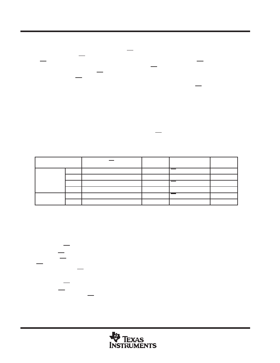
Table 1 lists the operational modes with respect to the state of CS, the number of I/O serial transfer clocks that
can be used, and the timing edge on which the MSB of the previous conversion appears at the output.
Table 1. Mode Operation
MODES
CS
NO. OF
I/O CLOCKS
MSB AT DATA OUT
TIMING
DIAGRAM
Mode 1
High between conversion cycles
10
CS falling edge
Figure 9
Fast Modes
Mode 2
Low continuously
10
EOC rising edge
Figure 10
Fast Modes
Mode 3
High between conversion cycles
11 to 16
CS falling edge
Figure 11
Mode 4
Low continuously
16
EOC rising edge
Figure 12
Slow Modes
Mode 5
High between conversion cycles
11 to 16
CS falling edge
Figure 13
Slow Modes
Mode 6
Low continuously
16
16th clock falling edge
Figure 14
These edges also initiate serial-interface communication.
No more than 16 clocks should be used.
fast modes
The device is in a fast mode when the serial I/O CLOCK data transfer is completed before the conversion is
completed. With a 10-clock serial transfer, the device can only run in a fast mode since a conversion does not
begin until the falling edge of the 10th I/O CLOCK.
mode 1: fast mode, CS inactive (high) between conversion cycles, 10-clock transfer
In this mode, CS is inactive (high) between serial I/O CLOCK transfers and each transfer is ten clocks long. The
falling edge of CS begins the sequence by removing DATA OUT from the high-impedance state. The rising edge
of CS ends the sequence by returning DATA OUT to the high-impedance state within the specified delay time.
Also, the rising edge of CS disables the I/O CLOCK and ADDRESS terminals within a setup time plus two falling
edges of the internal system clock.
mode 2: fast mode, CS active (low) continuously, 10-clock transfer
In this mode, CS is active (low) between serial I/O CLOCK transfers and each transfer is ten clocks long. After
the initial conversion cycle, CS is held active (low) for subsequent conversions; the rising edge of EOC then
begins each sequence by removing DATA OUT from the low logic level, allowing the MSB of the previous
conversion to appear immediately on this output.
相关PDF资料 |
PDF描述 |
|---|---|
| TLV1543CDBG4 | 11-CH 10-BIT SUCCESSIVE APPROXIMATION ADC, SERIAL ACCESS, PDSO20 |
| TLV1543CDBRG4 | 11-CH 10-BIT SUCCESSIVE APPROXIMATION ADC, SERIAL ACCESS, PDSO20 |
| TLV1543CFN | 11-CH 10-BIT SUCCESSIVE APPROXIMATION ADC, SERIAL ACCESS, PQCC20 |
| TLV1543IDB | 11-CH 10-BIT SUCCESSIVE APPROXIMATION ADC, SERIAL ACCESS, PDSO20 |
| TLV1543CN | 11-CH 10-BIT SUCCESSIVE APPROXIMATION ADC, SERIAL ACCESS, PDIP20 |
相关代理商/技术参数 |
参数描述 |
|---|---|
| TLV1543CDBRG4 | 功能描述:模数转换器 - ADC 10-Bit 200 kSPS Serial Out RoHS:否 制造商:Texas Instruments 通道数量:2 结构:Sigma-Delta 转换速率:125 SPs to 8 KSPs 分辨率:24 bit 输入类型:Differential 信噪比:107 dB 接口类型:SPI 工作电源电压:1.7 V to 3.6 V, 2.7 V to 5.25 V 最大工作温度:+ 85 C 安装风格:SMD/SMT 封装 / 箱体:VQFN-32 |
| TLV1543CDW | 功能描述:模数转换器 - ADC 10bit ADC w/11Chl RoHS:否 制造商:Texas Instruments 通道数量:2 结构:Sigma-Delta 转换速率:125 SPs to 8 KSPs 分辨率:24 bit 输入类型:Differential 信噪比:107 dB 接口类型:SPI 工作电源电压:1.7 V to 3.6 V, 2.7 V to 5.25 V 最大工作温度:+ 85 C 安装风格:SMD/SMT 封装 / 箱体:VQFN-32 |
| TLV1543CDWG4 | 功能描述:模数转换器 - ADC 10-Bit 200 kSPS Serial Out RoHS:否 制造商:Texas Instruments 通道数量:2 结构:Sigma-Delta 转换速率:125 SPs to 8 KSPs 分辨率:24 bit 输入类型:Differential 信噪比:107 dB 接口类型:SPI 工作电源电压:1.7 V to 3.6 V, 2.7 V to 5.25 V 最大工作温度:+ 85 C 安装风格:SMD/SMT 封装 / 箱体:VQFN-32 |
| TLV1543CDWR | 功能描述:模数转换器 - ADC 10-Bit 200 kSPS Serial Out RoHS:否 制造商:Texas Instruments 通道数量:2 结构:Sigma-Delta 转换速率:125 SPs to 8 KSPs 分辨率:24 bit 输入类型:Differential 信噪比:107 dB 接口类型:SPI 工作电源电压:1.7 V to 3.6 V, 2.7 V to 5.25 V 最大工作温度:+ 85 C 安装风格:SMD/SMT 封装 / 箱体:VQFN-32 |
| TLV1543CDWRG4 | 功能描述:模数转换器 - ADC 10-Bit 200 kSPS Serial Out RoHS:否 制造商:Texas Instruments 通道数量:2 结构:Sigma-Delta 转换速率:125 SPs to 8 KSPs 分辨率:24 bit 输入类型:Differential 信噪比:107 dB 接口类型:SPI 工作电源电压:1.7 V to 3.6 V, 2.7 V to 5.25 V 最大工作温度:+ 85 C 安装风格:SMD/SMT 封装 / 箱体:VQFN-32 |
发布紧急采购,3分钟左右您将得到回复。