- 您现在的位置:买卖IC网 > PDF目录67341 > TLV1548CDBRG4 (TEXAS INSTRUMENTS INC) 8-CH 10-BIT SUCCESSIVE APPROXIMATION ADC, SERIAL ACCESS, PDSO20 PDF资料下载
参数资料
| 型号: | TLV1548CDBRG4 |
| 厂商: | TEXAS INSTRUMENTS INC |
| 元件分类: | ADC |
| 英文描述: | 8-CH 10-BIT SUCCESSIVE APPROXIMATION ADC, SERIAL ACCESS, PDSO20 |
| 封装: | GREEN, PLASTIC, SSOP-20 |
| 文件页数: | 32/37页 |
| 文件大小: | 693K |
| 代理商: | TLV1548CDBRG4 |
第1页第2页第3页第4页第5页第6页第7页第8页第9页第10页第11页第12页第13页第14页第15页第16页第17页第18页第19页第20页第21页第22页第23页第24页第25页第26页第27页第28页第29页第30页第31页当前第32页第33页第34页第35页第36页第37页
TLV1544C, TLV1544I, TLV1548C, TLV1548I, TLV1548M
LOW-VOLTAGE 10-BIT ANALOG-TO-DIGITAL CONVERTERS
WITH SERIAL CONTROL AND 4/8 ANALOG INPUTS
SLAS139C – DECEMBER 1996 – REVISED JANUARY 1999
4
POST OFFICE BOX 655303
DALLAS, TEXAS 75265
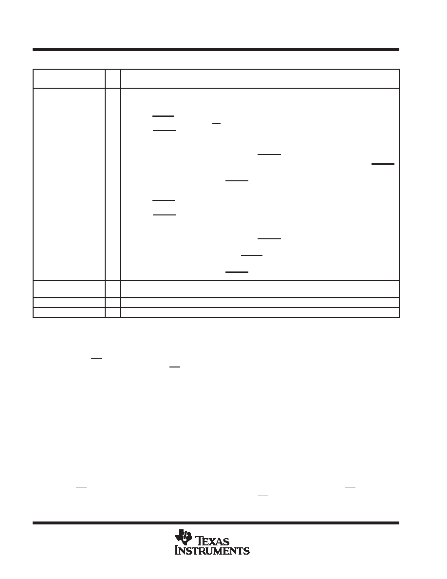
Terminal Functions (Continued)
TERMINAL
I/O
DESCRIPTION
NAME
NO.
I/O
DESCRIPTION
I/O CLK
3
18
I
Input/output clock. I/O CLK receives the serial I/O clock input in the two modes and performs the following
four functions in each mode:
Microprocessor mode
WhenINVCLK=V
CC, I/O CLK clocks the four input data bits into the input data register on the first four
rising edges of I/O CLK after CS
↓ with the multiplexer address available after the fourth rising edge.
When INV CLK = GND, input data bits are clocked in on the first four falling edges instead.
On the fourth falling edge of I/O CLK, the analog input voltage on the selected multiplex input begins
charging the capacitor array and continues to do so until the tenth rising edge of I/O CLK except in the
extended sampling cycle where the duration of CSTART determines when to end the sampling cycle.
Output data bits change on the first ten falling I/O clock edges regardless of the condition of INV CLK.
I/O CLK transfers control of the conversion to the internal state machine on the tenth rising edge of I/O
CLK regardless of the condition of INV CLK.
Digital signal processor (DSP) mode
WhenINVCLK=V
CC, I/O CLK clocks the four input data bits into the input data register on the first four
falling edges of I/O CLK after FS
↓ with the multiplexer address available after the fourth falling edges.
When INV CLK = GND, input data bits are clocked in on the first four rising edges instead.
On the fourth rising edge of I/O CLK, the analog input voltage on the selected multiplex input begins
charging the capacitor array and continues to do so until the tenth falling edge of I/O CLK except in the
extended sampling cycle where the duration of CSTART determines when to end the sampling cycle.
Output data MSB shows after FS↓and the rest of the output data bits change on the first ten rising I/O
CLK edges regarless of the condition of INV CLK.
I/OCLKtransferscontroloftheconversiontotheinternalstatemachineonthetenthfallingedgeofI/O
CLK regardless of the condition of INV CLK.
REF+
15
14
I
Upper reference voltage (nominally VCC ). The maximum input voltage range is determined by the difference
between the voltages applied to REF+ and REF–.
REF–
14
13
I
Lower reference voltage (nominally ground)
VCC
5
20
I
Positive supply voltage
Terminal numbers are for the D package.
Terminal numbers are for the DB, J, and FK packages.
detailed description
Initially, with CS high (inactive), DATA IN and I/O CLK are disabled and DATA OUT is in the high-impedance
state. When the serial interface takes CS low (active), the conversion sequence begins with the enabling of I/O
CLK and DATA IN and the removal of DATA OUT from the high-impedance state. The host then provides the
4-bit channel address to DATA IN and the I/O clock sequence to I/O CLK. During this transfer, the host serial
interface also receives the previous conversion result from DATA OUT. I/O CLK receives an input sequence from
the host that is from 10 to 16 clocks long. The first four valid I/O CLK cycles load the input data register with the
4-bit input data on DATA IN that selects the desired analog channel. The next six clock cycles provide the control
timing for sampling the analog input. Sampling of the analog input is held after the first valid I/O CLK sequence
of ten clocks. The tenth clock edge also takes EOC low and begins the conversion. The exact locations of the
I/O clock edges depend on the mode of operation.
serial interface
The TLV1548 is compatible with generic microprocessor serial interfaces such as SPI and QSPI, and a TMS320
DSP serial interface. The internal latched flag If_mode is generated by sampling the state of FS at the falling
edge of CS. If_mode is set to one (for microprocessor) when FS is high at the falling edge of CS, and If_mode
is cleared to zero (for DSP) when FS is low at the falling edge of CS. This flag controls the multiplexing of I/O
CLK and the state machine reset function. FS is pulled high when interfacing with a microprocessor.
相关PDF资料 |
PDF描述 |
|---|---|
| TLV1544IPW | 4-CH 10-BIT SUCCESSIVE APPROXIMATION ADC, SERIAL ACCESS, PDSO16 |
| TLV1544CD | 4-CH 10-BIT SUCCESSIVE APPROXIMATION ADC, SERIAL ACCESS, PDSO16 |
| TLV1544CDR | 4-CH 10-BIT SUCCESSIVE APPROXIMATION ADC, SERIAL ACCESS, PDSO16 |
| TLV1544IDR | 4-CH 10-BIT SUCCESSIVE APPROXIMATION ADC, SERIAL ACCESS, PDSO16 |
| TLV1544CPWR | 4-CH 10-BIT SUCCESSIVE APPROXIMATION ADC, SERIAL ACCESS, PDSO16 |
相关代理商/技术参数 |
参数描述 |
|---|---|
| TLV1548-EP | 制造商:TI 制造商全称:Texas Instruments 功能描述:LOW-VOLTAGE 10-BIT ANALOG-TO-DIGITAL CONVERTER WITH SERIAL CONTROL AND 8 ANALOG INPUTS |
| TLV1548I | 制造商:TI 制造商全称:Texas Instruments 功能描述:LOW-VOLTAGE 10-BIT ANALOG-TO-DIGITAL CONVERTERS WITH SERIAL CONTROL AND 4/8 ANALOG INPUTS |
| TLV1548IDB | 功能描述:模数转换器 - ADC 10bit A/D w/DSP Int RoHS:否 制造商:Texas Instruments 通道数量:2 结构:Sigma-Delta 转换速率:125 SPs to 8 KSPs 分辨率:24 bit 输入类型:Differential 信噪比:107 dB 接口类型:SPI 工作电源电压:1.7 V to 3.6 V, 2.7 V to 5.25 V 最大工作温度:+ 85 C 安装风格:SMD/SMT 封装 / 箱体:VQFN-32 |
| TLV1548IDBG4 | 功能描述:模数转换器 - ADC 10-Bit 85 kSPS Serial Out RoHS:否 制造商:Texas Instruments 通道数量:2 结构:Sigma-Delta 转换速率:125 SPs to 8 KSPs 分辨率:24 bit 输入类型:Differential 信噪比:107 dB 接口类型:SPI 工作电源电压:1.7 V to 3.6 V, 2.7 V to 5.25 V 最大工作温度:+ 85 C 安装风格:SMD/SMT 封装 / 箱体:VQFN-32 |
| TLV1548IDBR | 功能描述:模数转换器 - ADC 10-Bit 85 kSPS Serial Out RoHS:否 制造商:Texas Instruments 通道数量:2 结构:Sigma-Delta 转换速率:125 SPs to 8 KSPs 分辨率:24 bit 输入类型:Differential 信噪比:107 dB 接口类型:SPI 工作电源电压:1.7 V to 3.6 V, 2.7 V to 5.25 V 最大工作温度:+ 85 C 安装风格:SMD/SMT 封装 / 箱体:VQFN-32 |
发布紧急采购,3分钟左右您将得到回复。