- 您现在的位置:买卖IC网 > PDF目录385933 > TLV2322Y (Texas Instruments, Inc.) LinCMOSE LOW-VOLTAGE LOW-POWER OPERATIONAL AMPLIFIERS PDF资料下载
参数资料
| 型号: | TLV2322Y |
| 厂商: | Texas Instruments, Inc. |
| 英文描述: | LinCMOSE LOW-VOLTAGE LOW-POWER OPERATIONAL AMPLIFIERS |
| 中文描述: | LinCMOSE低压低功耗运算放大器 |
| 文件页数: | 2/33页 |
| 文件大小: | 502K |
| 代理商: | TLV2322Y |
第1页当前第2页第3页第4页第5页第6页第7页第8页第9页第10页第11页第12页第13页第14页第15页第16页第17页第18页第19页第20页第21页第22页第23页第24页第25页第26页第27页第28页第29页第30页第31页第32页第33页
TLV2322, TLV2322Y, TLV2324, TLV2324Y
LinCMOS
LOW-VOLTAGE LOW-POWER
OPERATIONAL AMPLIFIERS
SLOS187 – FEBRUARY 1997
2
POST OFFICE BOX 655303
DALLAS, TEXAS 75265
description (continued)
Low-voltage and low-power operation has been made possible by using the Texas Instruments silicon-gate
LinCMOS technology. The LinCMOS process also features extremely high input impedance and ultra-low bias
currents making these amplifiers ideal for interfacing to high-impedance sources such as sensor circuits or filter
applications.
To facilitate the design of small portable equipment, the TLV232x is made available in a wide range of package
options, including the small-outline and thin-shrink small-outline packages (TSSOP). The TSSOP package has
significantly reduced dimensions compared to a standard surface-mount package. Its maximum height of only
1.1 mm makes it particularly attractive when space is critical.
The device inputs and outputs are designed to withstand –100-mA currents without sustaining latch-up. The
TLV232x incorporates internal ESD-protection circuits that prevent functional failures at voltages up to 2000 V
as tested under MIL-STD 883C, Method 3015.2; however, care should be exercised in handling these devices
as exposure to ESD can result in the degradation of the device parametric performance.
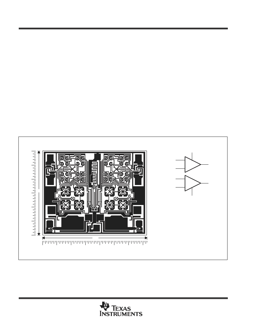
TLV2322Y chip information
This chip, when properly assembled, displays characteristics similar to the TLV2322I. Thermal compression or
ultrasonic bonding may be used on the doped-aluminum bonding pads. Chips may be mounted with conductive
epoxy or a gold-silicon preform.
BONDING PAD ASSIGNMENTS
CHIP THICKNESS: 15 MILS TYPICAL
BONDING PADS: 4
×
4 MILS MINIMUM
TJmax = 150
°
C
TOLERANCES ARE
±
10%.
ALL DIMENSIONS ARE IN MILS.
+
–
1OUT
1IN+
1IN–
VDD
VDD–/GND
(8)
(3)
(2)
(4)
+
–
2OUT
2IN+
2IN–
(5)
(6)
59
72
(5)
(4)
(3)
(2)
(6)
(7)
(8)
(1)
相关PDF资料 |
PDF描述 |
|---|---|
| TLV2324Y | Inductive DC |
| TLV2341(中文) | LINCMOS<TM> Programmable Low-Voltage OP AMP(电源电流可编程,低电压运放) |
| TLV2342(中文) | Dual LINCMOS<TM> Programmable Low-Voltage OP AMP(LICMOS,低电压,高速双运放) |
| TLV2342Y | LinCMOSE LOW-VOLTAGE HIGH-SPEED OPERATIONAL AMPLIFIERS |
| TLV2344ID | LinCMOSE LOW-VOLTAGE HIGH-SPEED OPERATIONAL AMPLIFIERS |
相关代理商/技术参数 |
参数描述 |
|---|---|
| TLV2324 | 制造商:TI 制造商全称:Texas Instruments 功能描述:LinCMOSE LOW-VOLTAGE LOW-POWER OPERATIONAL AMPLIFIERS |
| TLV2324ID | 功能描述:运算放大器 - 运放 Quad LiNCMOS RoHS:否 制造商:STMicroelectronics 通道数量:4 共模抑制比(最小值):63 dB 输入补偿电压:1 mV 输入偏流(最大值):10 pA 工作电源电压:2.7 V to 5.5 V 安装风格:SMD/SMT 封装 / 箱体:QFN-16 转换速度:0.89 V/us 关闭:No 输出电流:55 mA 最大工作温度:+ 125 C 封装:Reel |
| TLV2324IDG4 | 功能描述:运算放大器 - 运放 Quad LiNCMOS RoHS:否 制造商:STMicroelectronics 通道数量:4 共模抑制比(最小值):63 dB 输入补偿电压:1 mV 输入偏流(最大值):10 pA 工作电源电压:2.7 V to 5.5 V 安装风格:SMD/SMT 封装 / 箱体:QFN-16 转换速度:0.89 V/us 关闭:No 输出电流:55 mA 最大工作温度:+ 125 C 封装:Reel |
| TLV2324IDR | 功能描述:运算放大器 - 运放 Quad Lo-Vltg Mcrpwr Op Amp RoHS:否 制造商:STMicroelectronics 通道数量:4 共模抑制比(最小值):63 dB 输入补偿电压:1 mV 输入偏流(最大值):10 pA 工作电源电压:2.7 V to 5.5 V 安装风格:SMD/SMT 封装 / 箱体:QFN-16 转换速度:0.89 V/us 关闭:No 输出电流:55 mA 最大工作温度:+ 125 C 封装:Reel |
| TLV2324IDRG4 | 功能描述:运算放大器 - 运放 Quad Lo-Vltg Mcrpwr Op Amp RoHS:否 制造商:STMicroelectronics 通道数量:4 共模抑制比(最小值):63 dB 输入补偿电压:1 mV 输入偏流(最大值):10 pA 工作电源电压:2.7 V to 5.5 V 安装风格:SMD/SMT 封装 / 箱体:QFN-16 转换速度:0.89 V/us 关闭:No 输出电流:55 mA 最大工作温度:+ 125 C 封装:Reel |
发布紧急采购,3分钟左右您将得到回复。