- 您现在的位置:买卖IC网 > PDF目录385933 > TLV2322Y (Texas Instruments, Inc.) LinCMOSE LOW-VOLTAGE LOW-POWER OPERATIONAL AMPLIFIERS PDF资料下载
参数资料
| 型号: | TLV2322Y |
| 厂商: | Texas Instruments, Inc. |
| 英文描述: | LinCMOSE LOW-VOLTAGE LOW-POWER OPERATIONAL AMPLIFIERS |
| 中文描述: | LinCMOSE低压低功耗运算放大器 |
| 文件页数: | 25/33页 |
| 文件大小: | 502K |
| 代理商: | TLV2322Y |
第1页第2页第3页第4页第5页第6页第7页第8页第9页第10页第11页第12页第13页第14页第15页第16页第17页第18页第19页第20页第21页第22页第23页第24页当前第25页第26页第27页第28页第29页第30页第31页第32页第33页
TLV2322, TLV2322Y, TLV2324, TLV2324Y
LinCMOS
LOW-VOLTAGE LOW-POWER
OPERATIONAL AMPLIFIERS
SLOS187 – FEBRUARY 1997
25
POST OFFICE BOX 655303
DALLAS, TEXAS 75265
APPLICATION INFORMATION
single-supply operation (continued)
The TLV232x works well in conjunction with digital logic; however, when powering both linear devices and digital
logic from the same power supply, the following precautions are recommended:
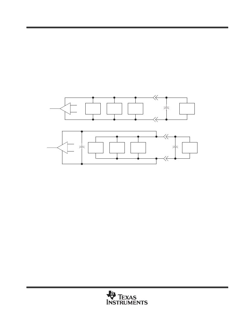
Power the linear devices from separate bypassed supply lines (see Figure 41); otherwise, the linear
device supply rails can fluctuate due to voltage drops caused by high switching currents in the digital
logic.
Use proper bypass techniques to reduce the probability of noise-induced errors. Single capacitive
decoupling is often adequate; however, RC decoupling may be necessary in high-frequency
applications.
–
+
Logic
Logic
Logic
Power
Supply
–
+
Logic
Logic
Logic
Power
Supply
(a) COMMON-SUPPLY RAILS
(b) SEPARATE-BYPASSED SUPPLY RAILS (preferred)
Figure 41. Common Versus Separate Supply Rails
input characteristics
The TLV232x is specified with a minimum and a maximum input voltage that, if exceeded at either input, could
cause the device to malfunction. Exceeding this specified range is a common problem, especially in
single-supply operation. The lower the range limit includes the negative rail, while the upper range limit is
specified at V
DD
– 1 V at T
A
= 25
°
C and at V
DD
– 1.2 V at all other temperatures.
The use of the polysilicon-gate process and the careful input circuit design gives the TLV232x very good input
offset voltage drift characteristics relative to conventional metal-gate processes. Offset voltage drift in CMOS
devices is highly influenced by threshold voltage shifts caused by polarization of the phosphorus dopant
implanted in the oxide. Placing the phosphorus dopant in a conductor (such as a polysilicon gate) alleviates the
polarization problem, thus reducing threshold voltage shifts by more than an order of magnitude. The offset
voltage drift with time has been calculated to be typically 0.1
μ
V/month, including the first month of operation.
Because of the extremely high input impedance and resulting low bias-current requirements, the TLV232x is
well suited for low-level signal processing; however, leakage currents on printed-circuit boards and sockets can
easily exceed bias-current requirements and cause a degradation in device performance. It is good practice
to include guard rings around inputs (similar to those of Figure 38 in the Parameter Measurement Information
section). These guards should be driven from a low-impedance source at the same voltage level as the
common-mode input (see Figure 42).
The inputs of any unused amplifiers should be tied to ground to avoid possible oscillation.
相关PDF资料 |
PDF描述 |
|---|---|
| TLV2324Y | Inductive DC |
| TLV2341(中文) | LINCMOS<TM> Programmable Low-Voltage OP AMP(电源电流可编程,低电压运放) |
| TLV2342(中文) | Dual LINCMOS<TM> Programmable Low-Voltage OP AMP(LICMOS,低电压,高速双运放) |
| TLV2342Y | LinCMOSE LOW-VOLTAGE HIGH-SPEED OPERATIONAL AMPLIFIERS |
| TLV2344ID | LinCMOSE LOW-VOLTAGE HIGH-SPEED OPERATIONAL AMPLIFIERS |
相关代理商/技术参数 |
参数描述 |
|---|---|
| TLV2324 | 制造商:TI 制造商全称:Texas Instruments 功能描述:LinCMOSE LOW-VOLTAGE LOW-POWER OPERATIONAL AMPLIFIERS |
| TLV2324ID | 功能描述:运算放大器 - 运放 Quad LiNCMOS RoHS:否 制造商:STMicroelectronics 通道数量:4 共模抑制比(最小值):63 dB 输入补偿电压:1 mV 输入偏流(最大值):10 pA 工作电源电压:2.7 V to 5.5 V 安装风格:SMD/SMT 封装 / 箱体:QFN-16 转换速度:0.89 V/us 关闭:No 输出电流:55 mA 最大工作温度:+ 125 C 封装:Reel |
| TLV2324IDG4 | 功能描述:运算放大器 - 运放 Quad LiNCMOS RoHS:否 制造商:STMicroelectronics 通道数量:4 共模抑制比(最小值):63 dB 输入补偿电压:1 mV 输入偏流(最大值):10 pA 工作电源电压:2.7 V to 5.5 V 安装风格:SMD/SMT 封装 / 箱体:QFN-16 转换速度:0.89 V/us 关闭:No 输出电流:55 mA 最大工作温度:+ 125 C 封装:Reel |
| TLV2324IDR | 功能描述:运算放大器 - 运放 Quad Lo-Vltg Mcrpwr Op Amp RoHS:否 制造商:STMicroelectronics 通道数量:4 共模抑制比(最小值):63 dB 输入补偿电压:1 mV 输入偏流(最大值):10 pA 工作电源电压:2.7 V to 5.5 V 安装风格:SMD/SMT 封装 / 箱体:QFN-16 转换速度:0.89 V/us 关闭:No 输出电流:55 mA 最大工作温度:+ 125 C 封装:Reel |
| TLV2324IDRG4 | 功能描述:运算放大器 - 运放 Quad Lo-Vltg Mcrpwr Op Amp RoHS:否 制造商:STMicroelectronics 通道数量:4 共模抑制比(最小值):63 dB 输入补偿电压:1 mV 输入偏流(最大值):10 pA 工作电源电压:2.7 V to 5.5 V 安装风格:SMD/SMT 封装 / 箱体:QFN-16 转换速度:0.89 V/us 关闭:No 输出电流:55 mA 最大工作温度:+ 125 C 封装:Reel |
发布紧急采购,3分钟左右您将得到回复。