- 您现在的位置:买卖IC网 > PDF目录98252 > TLV320ADC3001IYZHR (TEXAS INSTRUMENTS INC) 2-CH 16-BIT PROPRIETARY METHOD ADC, SERIAL ACCESS, PBGA16 PDF资料下载
参数资料
| 型号: | TLV320ADC3001IYZHR |
| 厂商: | TEXAS INSTRUMENTS INC |
| 元件分类: | ADC |
| 英文描述: | 2-CH 16-BIT PROPRIETARY METHOD ADC, SERIAL ACCESS, PBGA16 |
| 封装: | GREEN, DSBGA-16 |
| 文件页数: | 15/81页 |
| 文件大小: | 836K |
| 代理商: | TLV320ADC3001IYZHR |
第1页第2页第3页第4页第5页第6页第7页第8页第9页第10页第11页第12页第13页第14页当前第15页第16页第17页第18页第19页第20页第21页第22页第23页第24页第25页第26页第27页第28页第29页第30页第31页第32页第33页第34页第35页第36页第37页第38页第39页第40页第41页第42页第43页第44页第45页第46页第47页第48页第49页第50页第51页第52页第53页第54页第55页第56页第57页第58页第59页第60页第61页第62页第63页第64页第65页第66页第67页第68页第69页第70页第71页第72页第73页第74页第75页第76页第77页第78页第79页第80页第81页
LD(n)
LD (n+1)
2
1
0
3
0
3
2
1
3
RD(n)
LEFT CHANNEL
RIGHT CHANNEL
WORD
CLOCK
BIT
CLOCK
DATA
n-1 n-2 n-3
Ch_Offset_1 = 0
RD(n)
RD(n+1)
2
1
0
3
0
3
2
1
3
LD(n)
RIGHT CHANNEL
LEFT CHANNEL
WORD
CLOCK
BIT
CLOCK
DATA
n-1 n-2 n-3
Ch_Offset_1 = 0
Ch_Offset_2 = 3
RD(n)
RD(n+1)
2
1
0
3
0
3
2
1
3
LD(n)
RIGHT CHANNEL
LEFT CHANNEL
WORD
CLOCK
BIT
CLOCK
DATA
n-1 n-2 n-3
Ch_Offset_1 = 0
Ch_Offset_2 = 3
SLAS548C
– OCTOBER 2008 – REVISED APRIL 2011
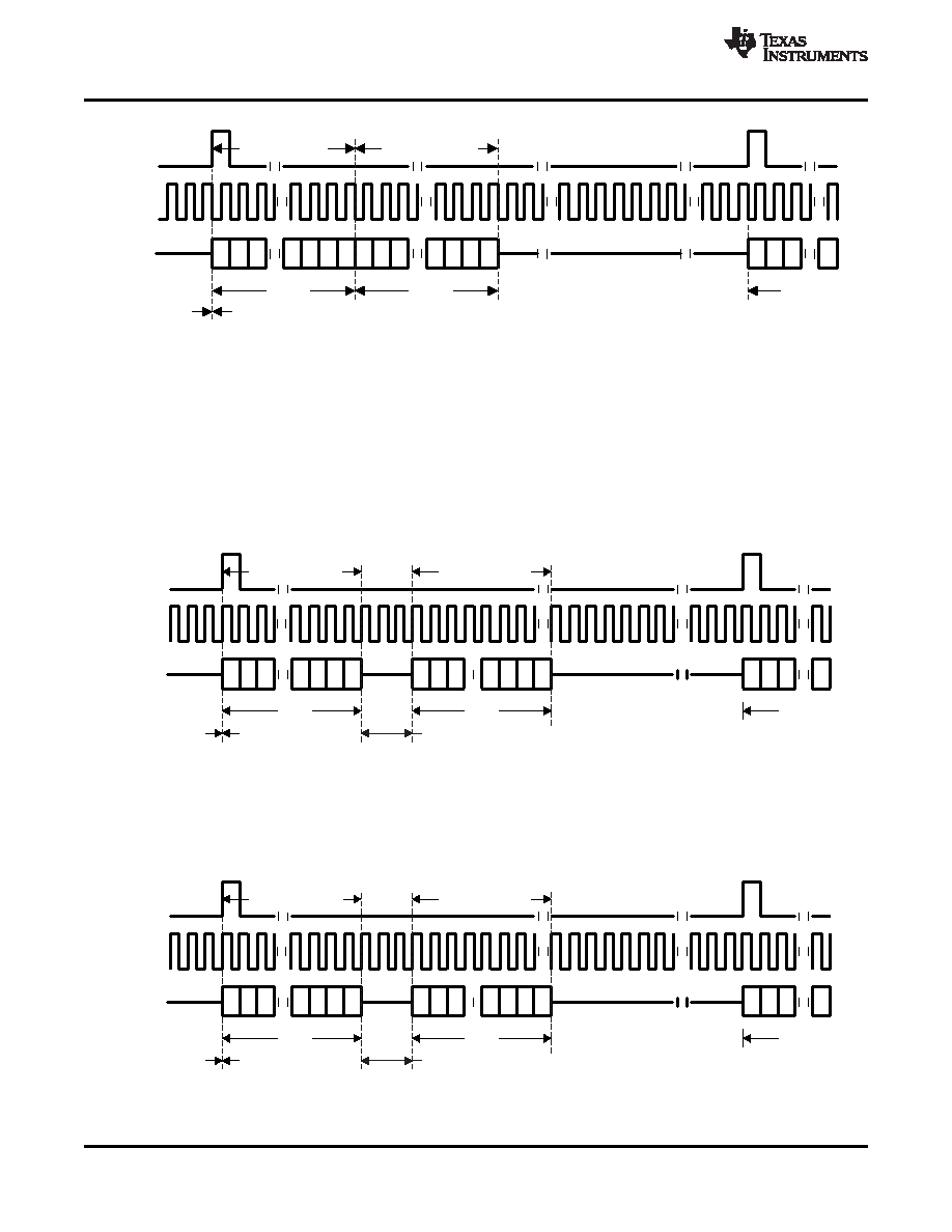
Figure 28. DSP Mode With Ch_Offset_1 = 0, Bit Clock Inverted
For DSP mode, the number of bit clocks per frame should be greater than twice the programmed word length of
the data. Also, the programmed offset value should be less than the number of bit clocks per frame by at least
the programmed word length of the data.
Figure 29 shows the DSP time-slot-based mode without channel swapping, and with Ch_Offset_1 = 0 and
Ch_Offset_2 = 3. The MSB of left channel data is valid on the first falling edge of the bit clock after the rising
edge of the word clock. Because the right channel has an offset of 3, the MSB of its data is valid on the third
falling edge of the bit clock after the LSB of the left-channel data. As in the case of other modes, the serial output
bus is put in the high-impedance state, if Hi-Z state operation of the output is enabled, during all the extra
bit-clock cycles in the frame.
Figure 29. DSP Mode, Time-Slot-Based Mode Enabled, Ch_Offset_1 = 0, Ch_Offset_2 = 3
Figure 30 shows the timing diagram for the DSP mode with left and right channels swapped, Ch_Offset_1 = 0,
and Ch_Offset_2 = 3. The MSB of the right channel is valid on the first falling edge of the bit clock after the rising
edge of the word clock. And, the MSB of the left channel is valid three bit-clock cycles after the LSB of right
channel, because the offset for the left channel is 3.
Figure 30. DSP Mode, Time-Slot-Based Mode Enabled, Ch_Offset_1 = 0, Ch_Offset_2 = 3, Channel Swap
Enabled
22
Copyright
2008–2011, Texas Instruments Incorporated
相关PDF资料 |
PDF描述 |
|---|---|
| TLV320ADC3101IRGER320 | SPECIALTY CONSUMER CIRCUIT, PQCC24 |
| TLV320ADC3101IRGET320 | SPECIALTY CONSUMER CIRCUIT, PQCC24 |
| TLV320ADC3101IRGER | SPECIALTY CONSUMER CIRCUIT, PQCC24 |
| TLV320ADC3101IRGET | SPECIALTY CONSUMER CIRCUIT, PQCC24 |
| TLV320AIC10C | SPECIALTY CONSUMER CIRCUIT, PQFP48 |
相关代理商/技术参数 |
参数描述 |
|---|---|
| TLV320ADC3001IYZHT | 功能描述:音频模/数转换器 IC 92dB 16b Low-Pwr Stereo ADC RoHS:否 制造商:Wolfson Microelectronics 转换速率: 分辨率: ADC 输入端数量: 工作电源电压: 最大工作温度: 最小工作温度: 安装风格: 封装 / 箱体: 封装: |
| TLV320ADC3001IYZHT | 制造商:Texas Instruments 功能描述:Analog/Digital (A/D) Converter IC |
| TLV320ADC3101 | 制造商:TI 制造商全称:Texas Instruments 功能描述:Low Power Stereo ADC for Wireless Handsets and Portable Audio |
| TLV320ADC3101EVM-K | 功能描述:音频 IC 开发工具 TLV320ADC3101EVM-K Eval Mod RoHS:否 制造商:Texas Instruments 产品:Evaluation Kits 类型:Audio Amplifiers 工具用于评估:TAS5614L 工作电源电压:12 V to 38 V |
| TLV320ADC3101IRGER | 功能描述:音频模/数转换器 IC 92dB (16B) Low Power Stereo ADC RoHS:否 制造商:Wolfson Microelectronics 转换速率: 分辨率: ADC 输入端数量: 工作电源电压: 最大工作温度: 最小工作温度: 安装风格: 封装 / 箱体: 封装: |
发布紧急采购,3分钟左右您将得到回复。