- 您现在的位置:买卖IC网 > PDF目录98254 > TLV320AIC33IZQER (TEXAS INSTRUMENTS INC) SPECIALTY CONSUMER CIRCUIT, PBGA80 PDF资料下载
参数资料
| 型号: | TLV320AIC33IZQER |
| 厂商: | TEXAS INSTRUMENTS INC |
| 元件分类: | 消费家电 |
| 英文描述: | SPECIALTY CONSUMER CIRCUIT, PBGA80 |
| 封装: | 5 X 5 MM, ROHS COMPLIANT, PLASTIC, VFBGA-80 |
| 文件页数: | 45/93页 |
| 文件大小: | 1427K |
| 代理商: | TLV320AIC33IZQER |
第1页第2页第3页第4页第5页第6页第7页第8页第9页第10页第11页第12页第13页第14页第15页第16页第17页第18页第19页第20页第21页第22页第23页第24页第25页第26页第27页第28页第29页第30页第31页第32页第33页第34页第35页第36页第37页第38页第39页第40页第41页第42页第43页第44页当前第45页第46页第47页第48页第49页第50页第51页第52页第53页第54页第55页第56页第57页第58页第59页第60页第61页第62页第63页第64页第65页第66页第67页第68页第69页第70页第71页第72页第73页第74页第75页第76页第77页第78页第79页第80页第81页第82页第83页第84页第85页第86页第87页第88页第89页第90页第91页第92页第93页
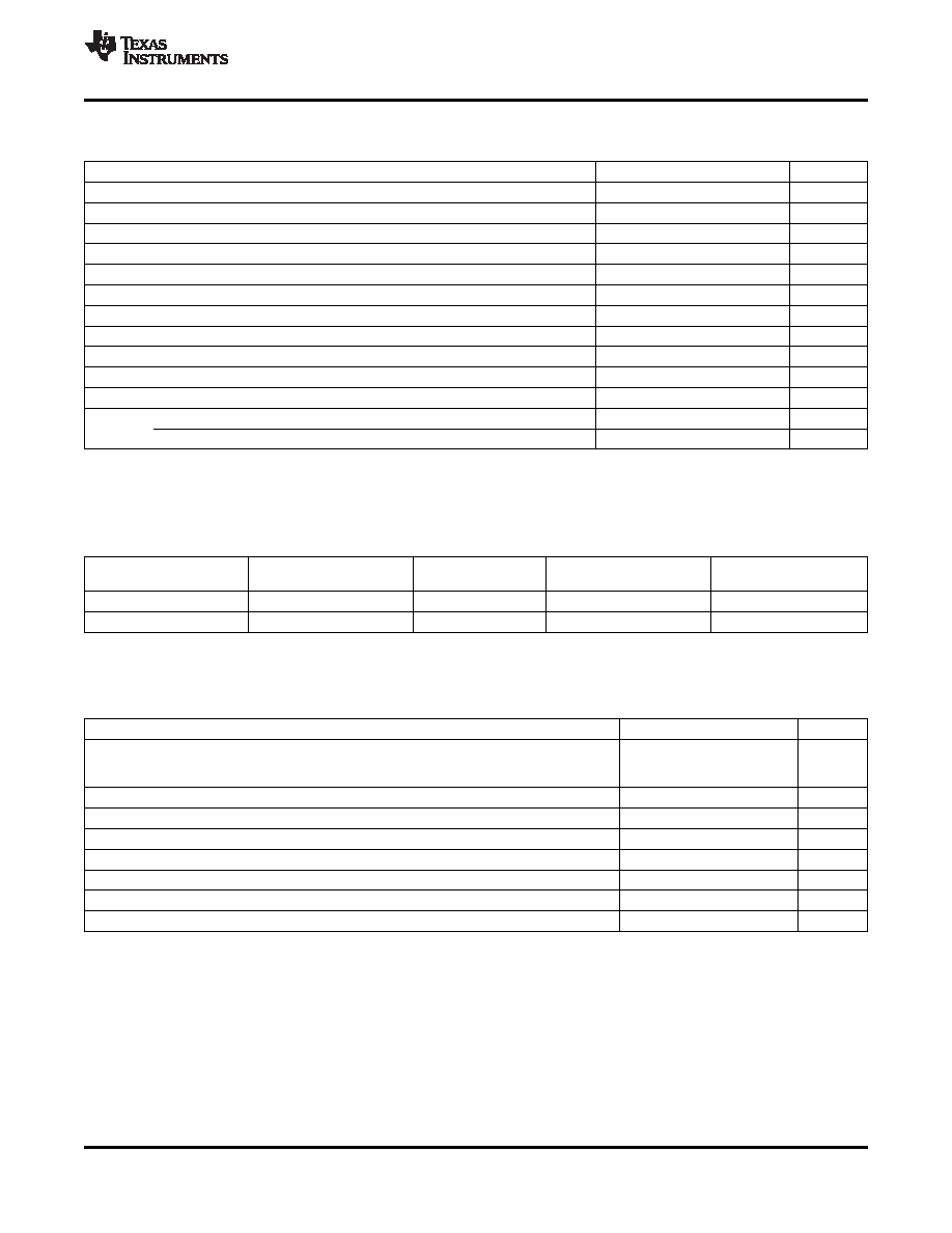
ABSOLUTE MAXIMUM RATINGS
DISSIPATION RATINGS
(1)
RECOMMENDED OPERATING CONDITIONS
www.ti.com ........................................................................................................................................... SLAS480B – JANUARY 2006 – REVISED DECEMBER 2008
over operating free-air temperature range (unless otherwise noted)
(1) (2)
VALUE
UNIT
AVDD to AVSS, DRVDD to DRVSS
–0.3 to 3.9
V
AVDD to DRVSS
–0.3 to 3.9
V
IOVDD to DVSS
–0.3 to 3.9
V
DVDD to DVSS
–0.3 to 2.5
V
AVDD to DRVDD
–0.1 to 0.1
V
Digital input voltage to DVSS
–0.3 V to IOVDD+0.3
V
Analog input voltage to AVSS
–0.3 V to AVDD+0.3
V
Operating temperature range
-40 to +85
°C
Storage temperature range
-65 to +105
°C
TJ Max
Junction temperature
105
°C
Power dissipation
(TJ Max – TA) / θJA
θ
JA
Thermal impedance , BGA package
63
°C/W
Thermal impedance, QFN package
38.5
°C/W
(1)
Stresses beyond those listed under absolute maximum ratings may cause permanent damage to the device. These are stress ratings
only, and functional operation of the device at these or any other conditions beyond those indicated under recommended operating
conditions is not implied. Exposure to absolute-maximum-rated conditions for extended periods may affect device reliability.
(2)
ESD complicance tested to EIA / JESD22-A114-B and passed.
TA = 25°C
TA = 75°C
TA = 85°C
PACKAGE TYPE
DERATING FACTOR
POWER RATING
BGA
1.27 W
15.9 mW/°C
476 mW
317 mW
QFN
2.08 W
26.0 mW/°C
779 mW
519 mW
(1)
This data was taken using 2 oz. trace and copper pad that is soldered directly to a JEDEC standard 4-layer 3 in × 3 in PCB.
over operating free-air temperature range (unless otherwise noted)
MIN
NOM
MAX
UNIT
AVDD,
Analog supply voltage
2.7
3.3
3.6
V
DRVDD1
/2(1)
DVDD(1)
Digital core supply voltage
1.65
1.8
1.95
V
IOVDD(1) Digital I/O supply voltage
1.1
1.8
3.6
V
VI
Analog full-scale 0 dB input voltage (DRVDD1 = 3.3 V)
0.707
VRMS
Stereo line-output load resistance
10
k
Stereo headphone-output load resistance
16
Digital output load capacitance
10
pF
TA
Operating free-air temperature
–40
85
°C
(1)
Analog voltage values are with respect to AVSS1, AVSS2, DRVSS; digital voltage values are with respect to DVSS.
Copyright 2006–2008, Texas Instruments Incorporated
5
Product Folder Link(s): TLV320AIC33
相关PDF资料 |
PDF描述 |
|---|---|
| TLV320AIC33IZQE | SPECIALTY CONSUMER CIRCUIT, PBGA80 |
| TLV320AIC33IRGZT | SPECIALTY CONSUMER CIRCUIT, PQCC48 |
| TLV320AIC33IRGZRG4 | SPECIALTY CONSUMER CIRCUIT, PQCC48 |
| TLV320AIC33IRGZTG4 | SPECIALTY CONSUMER CIRCUIT, PQCC48 |
| TLV320AIC33IRGZ | SPECIALTY CONSUMER CIRCUIT, PQCC48 |
相关代理商/技术参数 |
参数描述 |
|---|---|
| TLV320AIC33NIZQE | 制造商:Texas Instruments 功能描述: |
| TLV320AIC33NIZQER | 制造商:Texas Instruments 功能描述: |
| TLV320AIC33RHBRG4 | 制造商:Texas Instruments 功能描述:CODEC - Tape and Reel |
| TLV320AIC34 | 制造商:TI 制造商全称:Texas Instruments 功能描述:FOUR-CHANNEL, LOW-POWER AUDIO CODEC FOR PORTABLE AUDIO/TELEPHONY |
| TLV320AIC34_1 | 制造商:TI 制造商全称:Texas Instruments 功能描述:FOUR-CHANNEL, LOW-POWER AUDIO CODEC FOR PORTABLE AUDIO/TELEPHONY |
发布紧急采购,3分钟左右您将得到回复。