- 您现在的位置:买卖IC网 > PDF目录98255 > TLV5510IPWR (TEXAS INSTRUMENTS INC) 1-CH 8-BIT FLASH METHOD ADC, PARALLEL ACCESS, PDSO24 PDF资料下载
参数资料
| 型号: | TLV5510IPWR |
| 厂商: | TEXAS INSTRUMENTS INC |
| 元件分类: | ADC |
| 英文描述: | 1-CH 8-BIT FLASH METHOD ADC, PARALLEL ACCESS, PDSO24 |
| 封装: | PLASTIC, TSSOP-24 |
| 文件页数: | 6/20页 |
| 文件大小: | 330K |
| 代理商: | TLV5510IPWR |
TLV5510
2.7-V TO 3.6-V 8-BIT HIGH-SPEED ANALOG-TO-DIGITAL CONVERTER
SLAS124C– DECEMBER 1997 – REVISED DECEMBER 1999
14
POST OFFICE BOX 655303
DALLAS, TEXAS 75265
PRINCIPLES OF OPERATION
functional description (continued)
The MSB comparator block converts on the falling edge of each applied clock cycle. The LSB comparator blocks
CB-A and CB-B convert on the falling edges of the first and second following clock cycles, respectively. The
timing diagram of the conversion algorithm is shown in Figure 19.
analog input operation
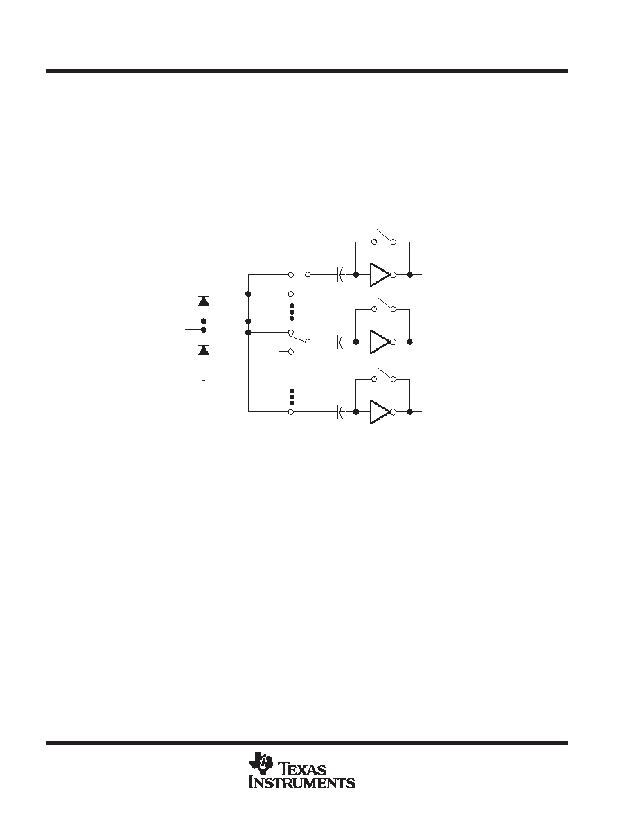
The analog input stage to the TLV5510 is a chopper-stabilized comparator and is equivalently shown below:
VDDA
ANALOG IN
S1
Vref(N)
φ1
φ2
S3
φ1
Cs
To Encoder Logic
φ2
S2
φ1
Cs
To Encoder Logic
φ2
S(N)
φ1
Cs
To Encoder Logic
Figure 20. External Connections for Using the Internal Reference Resistor Divider
Figure 20 depicts the analog input for the TLV5510. The switches shown are controlled by two internal clocks,
φ1 and φ2. These are nonoverlapping clocks that are generated from the CLK input. During the sampling period,
φ1, S1 is closed and the input signal is applied to one side of the sampling capacitor, Cs. Also during the sampling
period, S2 through S(N) are closed. This sets the comparator input to approximately 2.5 V. The delta voltage
is developed across Cs. During the comparison phase, φ2, S1 is switched to the appropriate reference voltage
for the bit value N, i.e., Vref(N). S2 is opened and Vref(N) – VCs toggles the comparator output to the appropriate
digital 1 or 0. The small resistance values for the switch, S1, and small value of the sampling capacitor combine
to produce the wide analog input bandwidth of the TLV5510. The source impedance driving the analog input
of the TLV5510 should be less than 100
across the range of input frequency spectrum.
reference inputs – REFB, REFT, REFBS, REFTS
The range of analog inputs that can be converted are determined by REFB and REFT, REFT being the
maximum reference voltage and REFB being the minimum reference voltage. The TLV5510 is tested with
REFT = 2.5 V or 2 V and REFB = 0.5 V or 0 V producing a 2-V full-scale range. The TLV5510 can operate with
REFT – REFB = 2.4 V, but the power dissipation in the reference resistor increases significantly (49 mW at 3.3 V
nominally). It is recommended that a 0.1
F capacitor be attached to REFB and REFT whether using externally
or internally generated voltages.
相关PDF资料 |
PDF描述 |
|---|---|
| TLV5510IPWLE | 1-CH 8-BIT FLASH METHOD ADC, PARALLEL ACCESS, PDSO24 |
| TLV5535IPWLE | 1-CH 8-BIT PROPRIETARY METHOD ADC, PARALLEL ACCESS, PDSO28 |
| TLV5535IPWRQ1 | 1-CH 8-BIT PROPRIETARY METHOD ADC, PARALLEL ACCESS, PDSO28 |
| TLV5535IPWRG4Q1 | 1-CH 8-BIT PROPRIETARY METHOD ADC, PARALLEL ACCESS, PDSO28 |
| TLV5535IPWR | 1-CH 8-BIT PROPRIETARY METHOD ADC, PARALLEL ACCESS, PDSO28 |
相关代理商/技术参数 |
参数描述 |
|---|---|
| TLV5535 | 制造商:TI 制造商全称:Texas Instruments 功能描述:8-BIT, 35 MSPS, LOW-POWER ANALOG-TO-DIGITAL CONVERTER |
| TLV5535EVM | 功能描述:数据转换 IC 开发工具 TLV5535 Eval Mod RoHS:否 制造商:Texas Instruments 产品:Demonstration Kits 类型:ADC 工具用于评估:ADS130E08 接口类型:SPI 工作电源电压:- 6 V to + 6 V |
| TLV5535IPW | 功能描述:模数转换器 - ADC 8bit 35Msps 1ch 3.3V RoHS:否 制造商:Texas Instruments 通道数量:2 结构:Sigma-Delta 转换速率:125 SPs to 8 KSPs 分辨率:24 bit 输入类型:Differential 信噪比:107 dB 接口类型:SPI 工作电源电压:1.7 V to 3.6 V, 2.7 V to 5.25 V 最大工作温度:+ 85 C 安装风格:SMD/SMT 封装 / 箱体:VQFN-32 |
| TLV5535IPWG4 | 功能描述:模数转换器 - ADC 8 Bit 35 MSPS Single Ch. Low Pwr RoHS:否 制造商:Texas Instruments 通道数量:2 结构:Sigma-Delta 转换速率:125 SPs to 8 KSPs 分辨率:24 bit 输入类型:Differential 信噪比:107 dB 接口类型:SPI 工作电源电压:1.7 V to 3.6 V, 2.7 V to 5.25 V 最大工作温度:+ 85 C 安装风格:SMD/SMT 封装 / 箱体:VQFN-32 |
| TLV5535IPWR | 功能描述:模数转换器 - ADC 8 Bit 35 MSPS Single Ch. Low Pwr RoHS:否 制造商:Texas Instruments 通道数量:2 结构:Sigma-Delta 转换速率:125 SPs to 8 KSPs 分辨率:24 bit 输入类型:Differential 信噪比:107 dB 接口类型:SPI 工作电源电压:1.7 V to 3.6 V, 2.7 V to 5.25 V 最大工作温度:+ 85 C 安装风格:SMD/SMT 封装 / 箱体:VQFN-32 |
发布紧急采购,3分钟左右您将得到回复。