- 您现在的位置:买卖IC网 > PDF目录19408 > TMS320C6414TBZLZA8 (Texas Instruments)IC FIXED-POINT DSP 532-FCBGA PDF资料下载
参数资料
| 型号: | TMS320C6414TBZLZA8 |
| 厂商: | Texas Instruments |
| 文件页数: | 9/146页 |
| 文件大小: | 0K |
| 描述: | IC FIXED-POINT DSP 532-FCBGA |
| 标准包装: | 60 |
| 系列: | TMS320C6414T/15T/16T |
| 类型: | 定点 |
| 接口: | 主机接口,McBSP,PCI,UTOPIA |
| 时钟速率: | 850MHz |
| 非易失内存: | 外部 |
| 芯片上RAM: | 1.03MB |
| 电压 - 输入/输出: | 3.30V |
| 电压 - 核心: | 1.20V |
| 工作温度: | -40°C ~ 105°C |
| 安装类型: | 表面贴装 |
| 封装/外壳: | 532-BFBGA,FCBGA |
| 供应商设备封装: | 532-FCBGA(23x23) |
| 包装: | 托盘 |
| 配用: | TMDXEVM6452-ND - TMDXEVM6452 296-23038-ND - DSP STARTER KIT FOR TMS320C6416 |
第1页第2页第3页第4页第5页第6页第7页第8页当前第9页第10页第11页第12页第13页第14页第15页第16页第17页第18页第19页第20页第21页第22页第23页第24页第25页第26页第27页第28页第29页第30页第31页第32页第33页第34页第35页第36页第37页第38页第39页第40页第41页第42页第43页第44页第45页第46页第47页第48页第49页第50页第51页第52页第53页第54页第55页第56页第57页第58页第59页第60页第61页第62页第63页第64页第65页第66页第67页第68页第69页第70页第71页第72页第73页第74页第75页第76页第77页第78页第79页第80页第81页第82页第83页第84页第85页第86页第87页第88页第89页第90页第91页第92页第93页第94页第95页第96页第97页第98页第99页第100页第101页第102页第103页第104页第105页第106页第107页第108页第109页第110页第111页第112页第113页第114页第115页第116页第117页第118页第119页第120页第121页第122页第123页第124页第125页第126页第127页第128页第129页第130页第131页第132页第133页第134页第135页第136页第137页第138页第139页第140页第141页第142页第143页第144页第145页第146页
TMS320C6414T, TMS320C6415T, TMS320C6416T
FIXEDPOINT DIGITAL SIGNAL PROCESSORS
SPRS226M NOVEMBER 2003 REVISED APRIL 2009
106
POST OFFICE BOX 1443
HOUSTON, TEXAS 772511443
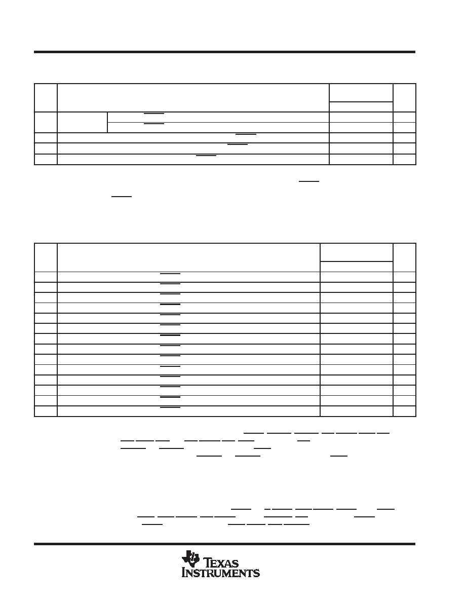
RESET TIMING
timing requirements for reset (see Figure 37)
NO.
600, 720,
850, 1G
UNIT
NO.
MIN
MAX
UNIT
1
tw(RST)
Width of the RESET pulse (PLL stable)
250
s
1
tw(RST)
Width of the RESET pulse (PLL needs to sync up)§
250
s
16
tsu(boot)
Setup time, boot configuration bits valid before RESET high
4E or 4C#
ns
17
th(boot)
Hold time, boot configuration bits valid after RESET high
4P
ns
18
tsu(PCLK-RSTH) Setup time, PCLK active before RESET high||
32N
ns
P = 1/CPU clock frequency in ns. For example, when running parts at 720 MHz, use P = 1.39 ns.
This parameter applies to CLKMODE x1 when CLKIN is stable, and applies to CLKMODE x6, x12, x20 when CLKIN and PLL are stable.
§ This parameter applies to CLKMODE x6, x12, x20 only (it does not apply to CLKMODE x1). The RESET signal is not connected internally to
the clock PLL circuit. The PLL, however, may need up to 250
s to stabilize following device power up or after PLL configuration has been
changed. During that time, RESET must be asserted to ensure proper device operation. See the clock PLL section for PLL lock times.
EMIFB address pins BEA[20:13, 11, 9:7] are the boot configuration pins during device reset.
# E = 1/AECLKIN clock frequency in ns. C = 1/CLKIN clock frequency in ns. Select whichever value is larger for the MIN parameter.
|| N = the PCI input clock (PCLK) period in ns. When PCI is enabled (PCI_EN = 1), this parameter must be met.
switching characteristics over recommended operating conditions during resetkh (see Figure 37)
NO.
PARAMETER
600, 720,
850, 1G
UNIT
NO.
PARAMETER
MIN
MAX
UNIT
2
td(RSTL-ECKI)
Delay time, RESET low to ECLKIN synchronized internally
2E
3P + 20E
ns
3
td(RSTH-ECKI)
Delay time, RESET high to ECLKIN synchronized internally
2E
16 070P
ns
4
td(RSTL-ECKO1HZ)
Delay time, RESET low to ECLKOUT1 high impedance
2E
ns
5
td(RSTH-ECKO1V)
Delay time, RESET high to ECLKOUT1 valid
16 070P
ns
6
td(RSTL-EMIFZHZ)
Delay time, RESET low to EMIF Z high impedance
2E
3P + 4E
ns
7
td(RSTH-EMIFZV)
Delay time, RESET high to EMIF Z valid
16E
16 070P
ns
8
td(RSTL-EMIFHIV)
Delay time, RESET low to EMIF high group invalid
2E
ns
9
td(RSTH-EMIFHV)
Delay time, RESET high to EMIF high group valid
16 070P
ns
10
td(RSTL-EMIFLIV)
Delay time, RESET low to EMIF low group invalid
2E
ns
11
td(RSTH-EMIFLV)
Delay time, RESET high to EMIF low group valid
16 070P
ns
12
td(RSTL-LOWIV)
Delay time, RESET low to low group invalid
0
ns
13
td(RSTH-LOWV)
Delay time, RESET high to low group valid
16 070P
ns
14
td(RSTL-ZHZ)
Delay time, RESET low to Z group high impedance
0
ns
15
td(RSTH-ZV)
Delay time, RESET high to Z group valid
2P
16 070P
ns
P = 1/CPU clock frequency in ns. For example, when running parts at 720 MHz, use P = 1.39 ns.
kE = the EMIF input clock (ECLKIN, CPU/4 clock, or CPU/6 clock) period in ns for EMIFA or EMIFB.
hEMIF Z group consists of:
AEA[22:3], BEA[20:1], AED[63:0], BED[15:0], CE[3:0], ABE[7:0], BBE[1:0], ARE/SDCAS/SADS/SRE,
AWE/SDWE/SWE, and AOE/SDRAS/SOE, SOE3, ASDCKE, and PDT.
EMIF high group consists of: AHOLDA and BHOLDA (when the corresponding HOLD input is high)
EMIF low group consists of:
ABUSREQ and BBUSREQ; AHOLDA and BHOLDA (when the corresponding HOLD input is low)
Low group consists of:
XSP_CS, CLKX2/XSP_CLK, and DX2/XSP_DO; all of which apply only when PCI EEPROM (BEA13)
is enabled (with PCI_EN = 1 and MCBSP2_EN = 0). Otherwise, the CLKX2/XSP_CLK and DX2/XSP_DO
pins are in the Z group. For more details on the PCI configuration pins, see the Device Configurations section
of this data sheet.
Z group consists of:
HD[31:0]/AD[31:0], CLKX0, CLKX1/URADDR4, CLKX2/XSP_CLK, FSX0, FSX1/UXADDR3, FSX2, DX0,
DX1/UXADDR4, DX2/XSP_DO, CLKR0, CLKR1/URADDR2, CLKR2, FSR0, FSR1/UXADDR2, FSR2,
TOUT0, TOUT1, TOUT2, GP[8:0], GP10/PCBE3, HR/W/PCBE2, HDS2/PCBE1, PCBE0, GP13/PINTA,
GP11/PREQ, HDS1/PSERR, HCS/PPERR, HCNTL1/PDEVSEL, HAS/PPAR, HCNTL0/PSTOP,
HHWIL/PTRDY (16-bit HPI mode only), HRDY/PIRDY, HINT/PFRAME, UXDATA[7:0], UXSOC, UXCLAV,
and URCLAV.
相关PDF资料 |
PDF描述 |
|---|---|
| VE-JNY-IZ | CONVERTER MOD DC/DC 3.3V 16.5W |
| REC3-053.3SRW/H2/A | CONV DC/DC 3W 4.5-9VIN 3.3VOUT |
| RMC40DRTS-S734 | CONN EDGECARD 80POS DIP .100 SLD |
| HMC28DRYS-S734 | CONN EDGECARD 56POS DIP .100 SLD |
| RCB105DHFR | CONN EDGECARD 210POS .050 SMD |
相关代理商/技术参数 |
参数描述 |
|---|---|
| TMS320C6414TBZLZW8 | 制造商:Rochester Electronics LLC 功能描述:- Bulk |
| TMS320C6414TGLZ1 | 制造商:Rochester Electronics LLC 功能描述: 制造商:Texas Instruments 功能描述: |
| TMS320C6414TGLZ6 | 制造商:Rochester Electronics LLC 功能描述:FIXED-POINT DIGITAL SIGNAL PROCESSOR - Bulk 制造商:Texas Instruments 功能描述: |
| TMS320C6414TGLZ7 | 功能描述:数字信号处理器和控制器 - DSP, DSC Fixed-Pt Dig Sig Proc RoHS:否 制造商:Microchip Technology 核心:dsPIC 数据总线宽度:16 bit 程序存储器大小:16 KB 数据 RAM 大小:2 KB 最大时钟频率:40 MHz 可编程输入/输出端数量:35 定时器数量:3 设备每秒兆指令数:50 MIPs 工作电源电压:3.3 V 最大工作温度:+ 85 C 封装 / 箱体:TQFP-44 安装风格:SMD/SMT |
| TMS320C6414TGLZ8 | 制造商:Rochester Electronics LLC 功能描述:FIXED-POINT DIGITAL SIGNAL PROCESSOR - Bulk 制造商:Texas Instruments 功能描述: |
发布紧急采购,3分钟左右您将得到回复。