- 您现在的位置:买卖IC网 > PDF目录382627 > TMX320R2812ZHHQ (Texas Instruments, Inc.) TMS320R2811, TMS320R2812 Digital Signal Processors PDF资料下载
参数资料
| 型号: | TMX320R2812ZHHQ |
| 厂商: | Texas Instruments, Inc. |
| 元件分类: | 数字信号处理 |
| 英文描述: | TMS320R2811, TMS320R2812 Digital Signal Processors |
| 中文描述: | TMS320R2811,TMS320R2812数字信号处理器 |
| 文件页数: | 93/147页 |
| 文件大小: | 2021K |
| 代理商: | TMX320R2812ZHHQ |
第1页第2页第3页第4页第5页第6页第7页第8页第9页第10页第11页第12页第13页第14页第15页第16页第17页第18页第19页第20页第21页第22页第23页第24页第25页第26页第27页第28页第29页第30页第31页第32页第33页第34页第35页第36页第37页第38页第39页第40页第41页第42页第43页第44页第45页第46页第47页第48页第49页第50页第51页第52页第53页第54页第55页第56页第57页第58页第59页第60页第61页第62页第63页第64页第65页第66页第67页第68页第69页第70页第71页第72页第73页第74页第75页第76页第77页第78页第79页第80页第81页第82页第83页第84页第85页第86页第87页第88页第89页第90页第91页第92页当前第93页第94页第95页第96页第97页第98页第99页第100页第101页第102页第103页第104页第105页第106页第107页第108页第109页第110页第111页第112页第113页第114页第115页第116页第117页第118页第119页第120页第121页第122页第123页第124页第125页第126页第127页第128页第129页第130页第131页第132页第133页第134页第135页第136页第137页第138页第139页第140页第141页第142页第143页第144页第145页第146页第147页
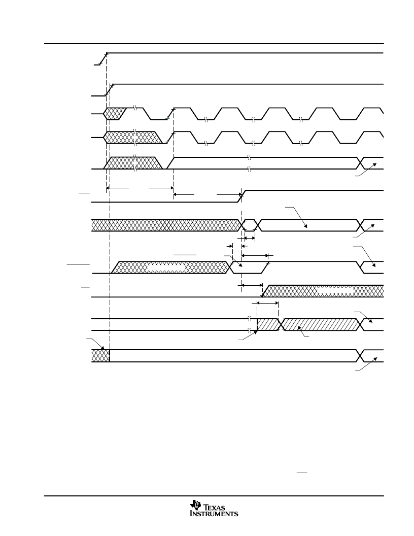
Electrical Specifications
93
June 2004
SPRS257
t
w(RSL1)
t
h(XPLLDIS)
t
h(XMP/MC)
t
h(boot-mode)
(
see Note C)
V
DDIO
, V
DDAn
,
V
DDAIO
(3.3 V)
(See Note A)
XCLKIN
2.5 V
0.3 V
X1
XRS
XF/XPLLDIS
XMP/MC
Boot-Mode Pins
V
DD
, V
DD1
(1.8 V (or 1.9 V))
XCLKOUT
I/O Pins
User-Code Dependent
User-Code Dependent
User-Code Dependent
Boot-ROM Execution Starts
Peripheral/GPIO Function
Based on Boot Code
GPIO Pins as Input
XPLLDIS Sampling
GPIOF14
XCLKIN/8 (See Note B)
GPIO Pins as Input (State Depends on Internal PU/PD)
t
OSCST
(Don’t Care)
(Don’t Care)
User-Code Dependent
Address/Data/
Control
Address/Data Valid. Internal Boot-ROM Code Execution Phase
User-Code Execution Phase
NOTES: A. V
DDAn
V
DDA1
/V
DDA2
and AV
DDREFBG
B. Upon power up, SYSCLKOUT is XCLKIN/2 if the PLL is enabled. Since both the XTIMCLK and CLKMODE bits in the
XINTCNF2 register come up with a reset state of 1, SYSCLKOUT is further divided by 4 before it appears at XCLKOUT. This
explains why XCLKOUT = XCLKIN/8 during this phase.
C. After reset, the Boot ROM code executes instructions for 1260 SYSCLKOUT cycles (SYSCLKOUT = XCLKIN/2) and then
samples BOOT Mode pins. Based on the status of the Boot Mode pin, the boot code branches to destination memory or boot
code function in ROM. The BOOT Mode pins should be held high/low for at least 2520 XCLKIN cycles from boot ROM
execution time for proper selection of Boot modes.
If Boot ROM code executes after power-on conditions (in debugger environment), the Boot code execution time is based on
the current SYSCLKOUT speed. The SYSCLKOUT will be based on user environment and could be with or without PLL
enabled.
D. The state of the GPIO pins is undefined (i.e., they could be input or output) until the 1.8-V (or 1.9-V) supply reaches at least
1 V and 3.3-V supply reaches 2.5 V.
t
d(EX)
See Note D
t
su(XPLLDIS)
Figure 6
6. Power-on Reset in Microcomputer Mode (XMP/MC = 0)
A
相关PDF资料 |
PDF描述 |
|---|---|
| TMX320R2812ZHHS | TMS320R2811, TMS320R2812 Digital Signal Processors |
| TMP320R2811ZHHA | TMS320R2811, TMS320R2812 Digital Signal Processors |
| TMP320R2811ZHHQ | TMS320R2811, TMS320R2812 Digital Signal Processors |
| TMP320R2811ZHHS | TMS320R2811, TMS320R2812 Digital Signal Processors |
| TMP320R2812GHHA | TMS320R2811, TMS320R2812 Digital Signal Processors |
相关代理商/技术参数 |
参数描述 |
|---|---|
| TMX320R2812ZHHS | 制造商:TI 制造商全称:Texas Instruments 功能描述:TMS320R2811, TMS320R2812 Digital Signal Processors |
| TMX320TCI100BGLZ7 | 制造商:Texas Instruments 功能描述: |
| TMX320TCI100GLZ | 制造商:Texas Instruments 功能描述: |
| TMX320TCI100ZLZ6 | 制造商:Texas Instruments 功能描述: |
| TMX320TCI100ZLZ6N | 制造商:Texas Instruments 功能描述: |
发布紧急采购,3分钟左右您将得到回复。