- 您现在的位置:买卖IC网 > PDF目录19664 > TNY265P (Power Integrations)IC OFFLINE SWIT OTP OCP HV 8DIP PDF资料下载
参数资料
| 型号: | TNY265P |
| 厂商: | Power Integrations |
| 文件页数: | 5/22页 |
| 文件大小: | 0K |
| 描述: | IC OFFLINE SWIT OTP OCP HV 8DIP |
| 标准包装: | 3,000 |
| 系列: | TinySwitch®-II |
| 输出隔离: | 隔离 |
| 频率范围: | 124kHz ~ 140kHz |
| 输出电压: | 700V |
| 功率(瓦特): | 11W |
| 工作温度: | -40°C ~ 150°C |
| 封装/外壳: | 8-DIP(0.300",7.62mm),7 引线 |
| 供应商设备封装: | DIP-8B |
| 包装: | 管件 |
�� �
�
�TNY263-268�
�the� appropriate� current� limit.� At� high� loads,� when� the� EN/UV�
�pin� is� high� (less� than� 240� μ� A� out� of� the� pin),� a� switching� cycle�
�with� the� full� current� limit� occurs.� At� lighter� loads,� when� EN/UV�
�reduced� even� further� (Figure� 9).� Only� a� small� percentage� of�
�cycles� will� occur� to� satisfy� the� power� consumption� of� the�
�power� supply.�
�is� high,� a� switching� cycle� with� a� reduced� current� limit� occurs.�
�The� response� time� of� the� TinySwitch-II� ON/OFF� control�
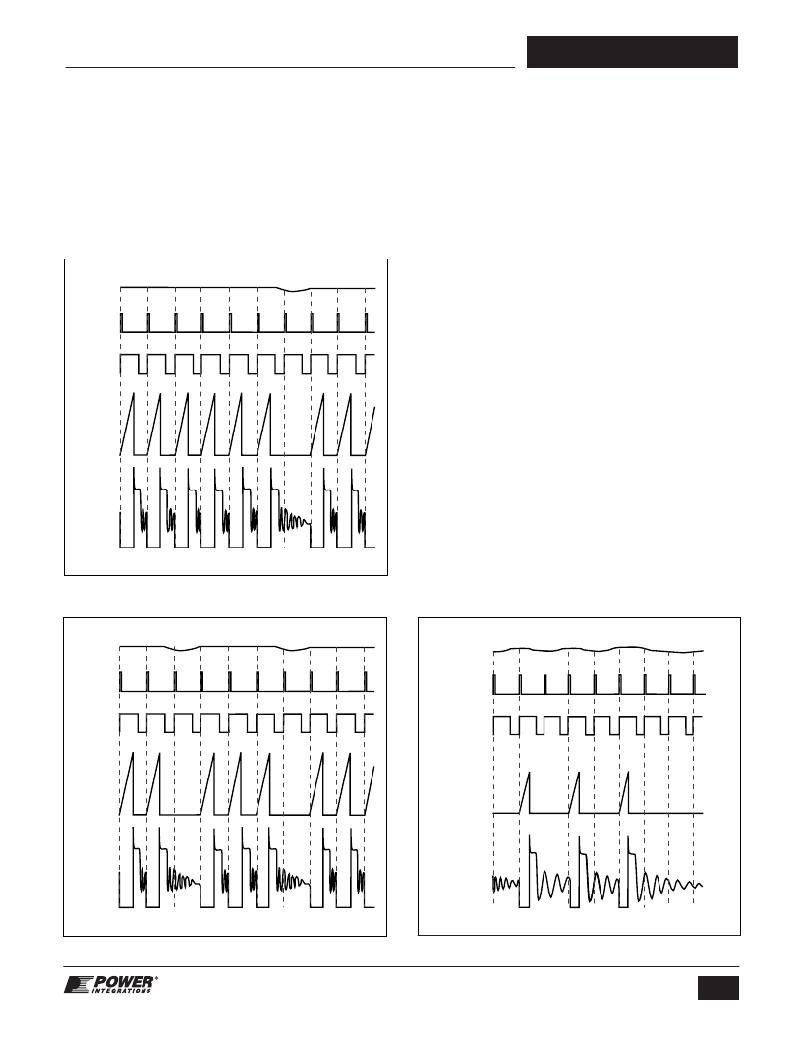
�At� near� maximum� load,� TinySwitch-II� will� conduct� during�
�nearly� all� of� its� clock� cycles� (Figure� 6).� At� slightly� lower� load,� it�
�will� “skip”� additional� cycles� in� order� to� maintain� voltage�
�regulation� at� the� power� supply� output� (Figure� 7).� At� medium�
�loads,� cycles� will� be� skipped� and� the� current� limit� will� be�
�reduced� (Figure� 8).� At� very� light� loads,� the� current� limit� will� be�
�V�
�EN�
�CLOCK�
�scheme� is� very� fast� compared� to� normal� PWM� control.� This�
�provides� tight� regulation� and� excellent� transient� response.�
�Power� Up/Down�
�The� TinySwitch-II� requires� only� a� 0.1� μ� F� capacitor� on� the�
�BYPASS� pin.� Because� of� its� small� size,� the� time� to� charge� this�
�capacitor� is� kept� to� an� absolute� minimum,� typically� 0.6� ms.�
�Due� to� the� fast� nature� of� the� ON/OFF� feedback,� there� is� no�
�overshoot� at� the� power� supply� output.� When� an� external�
�resistor� (2� M� Ω� )� is� connected� from� the� positive� DC� input� to� the�
�EN/UV� pin,� the� power� MOSFET� switching� will� be� delayed�
�during� power-up� until� the� DC� line� voltage� exceeds� the�
�threshold� (100� V).� Figures� 10� and� 11� show� the� power-up� timing�
�waveform� of� TinySwitch-II� in� applications� with� and� without� an�
�D�
�MAX�
�external� resistor� (2� M� Ω� )� connected� to� the� EN/UV� pin.�
�During� power-down,� when� an� external� resistor� is� used,� the�
�power� MOSFET� will� switch� for� 50� ms� after� the� output� loses�
�I� DRAIN�
�V� DRAIN�
�PI-2749-050301�
�regulation.� The� power� MOSFET� will� then� remain� off� without�
�any� glitches� since� the� undervoltage� function� prohibits� restart�
�when� the� line� voltage� is� low.�
�Figure� 12� illustrates� a� typical� power-down� timing� waveform� of�
�TinySwitch-II.� Figure� 13� illustrates� a� very� slow� power-down�
�timing� waveform� of� TinySwitch-II� as� in� standby� applications.�
�The� external� resistor� (2� M� Ω� )� is� connected� to� the� EN/UV� pin� in�
�this� case� to� prevent� unwanted� restarts.�
�The� TinySwitch-II� does� not� require� a� bias� winding� to� provide�
�power� to� the� chip,� because� it� draws� the� power� directly� from�
�Figure� 6.�
�V�
�EN�
�CLOCK�
�TinySwitch-II� Operation� at� Near� Maximum� Loading.�
�the� DRAIN� pin� (see� Functional� Description� above).� This� has�
�V�
�EN�
�CLOCK�
�D�
�MAX�
�D�
�MAX�
�I� DRAIN�
�V� DRAIN�
�PI-2667-090700�
�I� DRAIN�
�V� DRAIN�
�PI-2377-091100�
�Figure� 7.�
�TinySwitch-II� Operation� at� Moderately� Heavy� Loading.�
�Figure� 8.�
�TinySwitch-II� Operation� at� Medium� Loading.�
�5�
�www.powerint.com�
�Rev.� H� 02/09�
�相关PDF资料 |
PDF描述 |
|---|---|
| RW2-0509D/H2/B | CONV DC/DC 2W 4.5-9VIN +/-09VOUT |
| RW2-0505D/H2/B | CONV DC/DC 2W 4.5-9VIN +/-05VOUT |
| TNY265G-TL | IC OFFLINE SWIT OTP OCP HV 8SMD |
| VE-21Z-CW-F2 | CONVERTER MOD DC/DC 2V 40W |
| ATF1500A-10AC | IC CPLD 32 MACROCELL 10NS 44TQFP |
相关代理商/技术参数 |
参数描述 |
|---|---|
| TNY265PG | 功能描述:交流/直流开关转换器 7.5 W (85-265 VAC) 11 W (230 VAC) RoHS:否 制造商:STMicroelectronics 输出电压:800 V 输入/电源电压(最大值):23.5 V 输入/电源电压(最小值):11.5 V 开关频率:115 kHz 电源电流:1.6 mA 工作温度范围:- 40 C to + 150 C 安装风格:SMD/SMT 封装 / 箱体:SSO-10 封装:Reel |
| TNY265PN | 功能描述:交流/直流开关转换器 7.5W 85-265 VAC 11W/230 VAC RoHS:否 制造商:STMicroelectronics 输出电压:800 V 输入/电源电压(最大值):23.5 V 输入/电源电压(最小值):11.5 V 开关频率:115 kHz 电源电流:1.6 mA 工作温度范围:- 40 C to + 150 C 安装风格:SMD/SMT 封装 / 箱体:SSO-10 封装:Reel |
| TNY265PN-TL | 制造商:POWERINT 制造商全称:Power Integrations, Inc. 功能描述:Enhanced, Energy Efficient, Low Power Off-line Switcher |
| TNY265PTL | 制造商:POWERINT 制造商全称:Power Integrations, Inc. 功能描述:Enhanced, Energy Efficient, Low Power Off-line Switcher |
| TNY266 | 制造商:POWERINT 制造商全称:Power Integrations, Inc. 功能描述:Generic PCB for DVD Player using TinySwitch-II |
发布紧急采购,3分钟左右您将得到回复。